This thread has been locked.

If you have a related question, please click the "Ask a related question" button in the top right corner. The newly created question will be automatically linked to this question.

TPS552882: Deviation of Calculated inductor value from webench & design calc

Part Number: TPS552882

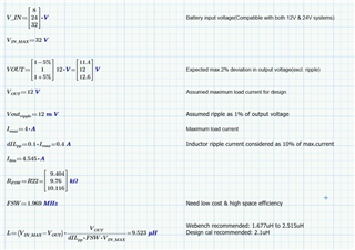
While performing WCCA, I've noticed that the calculated inductor(9.6uH-> Even at nominal values) is far less than the recommended value from both webench & excel calculator(max.2.5uH). Added the webench report here for your reference. 

 WBDesign35_Current limit 4.54A_1.8uH.pdf

Also, webench is mandatorily keeping one electrolytic capacitor at the input side(even though it's of low value-> <20uF). I was thinking to replace it with multiple ceramic capacitors as it provides better rms handling capacitor & low ESR value. Is it because of capacitance change due to bias voltage in ceramic? The battery will be kept atleast 1m from the actual PCB and we have load dump & EMI filter before this buck boost circuitry. 

  • Hi Santhosh,

    Thank you for reaching out. May I know what application the TPS552882 is used in?

    The 9.6uH result is calculated in buck mode, while the <2.5uH result is calculated in boost mode. Normally we think inductor current ripple =40% is ok. Why do you have 10% requirement?

    L=2.2uH, boost mode current ripple ratio:0.1 , buck mode current ripple ratio : 0.45

    L=9.6uH, boost mode current ripple ratio:0.02 , buck mode current ripple ratio : 0.1

    When use 9.6uH inductor, the right half plane zero in boost mode is low(20kHz), making it difficult for loop compensation.

    Also, do you have requirement about thermal performance, I am afraid that when Vin=8V, output 12V/4A, fsw=2MHz, the chip temperature would be high. Do you consider to use 400kHz?

    Regards,

    Mulin

  • Hi Mulin,

    Thanks for the detailed response. 

    We're using it for the automotive application(ambient temp: -40'C to 85'C) & we've metal casing with around 10mm distance from IC to metal plate. We'll perform thermal simulation post layout once to check the chip temperature. 

    I didn't know about ripple varying with buck & boost mode. Thanks for the detailed explanation, I'll calculate properly now. 

    We've space constraint so if we go with lower frequency then we won't be able to achieve the expected space efficiency. Also, we're trying to avoid choosing frequencies which overlaps with CISPR. 

    If you could tell me the possible reason behind selection of low value electrolytic capacitor then it would be really helpful. Can we replace those electrolytic caps with ceramic ones? as it will have better ESR & current handling capability. Is it something to do with ceramic capacitor variation with bias voltage?

  • Hi Santhosh,

    We need the output capacitor to reduce Vout ripple and for better load transient performance.  If the effective capacitance is too small , the voltage overshoot and undershoot will be large in transient conditions. Do you have any requirement about this? 

    If we replace electrolytic caps with ceramic ones, we need to consider effective capacitance with DC bias. So you need several times ceramic capacitors to compensate the effective capacitance reduce. Also, in low temperature, the effective capacitance will also change, make it difficult to design loop compensation. So I recommend to use a low ESR electrolytic cap. Please notify that in low temperature, the electrolytic cap ESR will increase. So the compensation parameters should be double checked in low temperature situation.

    Regards,

    Mulin