This thread has been locked.

If you have a related question, please click the "Ask a related question" button in the top right corner. The newly created question will be automatically linked to this question.

TPS54360: TPS54360DDAR chip damage

Part Number: TPS54360
Other Parts Discussed in Thread: LMR36015

Hi TI team  ,

We are using the chip TPS54360DDAR for generating -24V input from +24V .Recently we have observed from field that TPS54360DDAR  is Burning .its burning at Vin Pin (Pin no 2) and short B/w SW (Pin 8) and Gnd 
Initially its working fine(during production testing) after some time in the field its getting damaged (IC burn).From 2023 IC burn out issue is increased,so many IC's were burnt .We could see so many people have reported the same issue in TI forum ,but  could not see an exact solution.
We have started to find and analyse  the root  cause
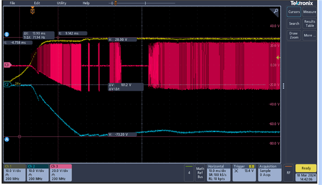
find the snapshot of design for your reference.
Please check the design and provide feedback on what could be the  cause of an  IC to burn 
When we evaluate we see that all of the failed boards are produced using TPS54360 batch 2031 (see the image below)
Boards are produced after Jan 2023 and used above components from batch 2031. There are no changes to the design or process we follow in our production thus no variability from our side.
Can you please go a little deeper in this investigation and find what has change happened from the IC production? Was there any PCN related to process/production house/material, etc?
We still have 1200 pcs stock from the above batch and we are afraid that failures will continue. Let us know how to mitigate this risk? If you can suggest some testing which can at least identify the bad ones in production itself also save from failure from the field. 
Also, 2500 pcs from another batch as well in stock (this we haven't used yet)
  • Hi Venkatesh,

    You are outside the specification of this device.

    The max operating input voltage is 36V and its absmax is 42.

    With respect to IC ground, you have a 48V input.

    Please consider an alternative device for this design like LMR36015 which is rated for 60V.

  • Hi Marshall, 

    Thanks for the quick reply. I am  bit confused. As per datasheet the absolute maximum voltage of input pin is 65V and recommend maximum operating voltage is 60V .As per circuit voltage on the input pin is 48v with respect to IC Ground (-24V) 

    Attached screeshot of datasheet TPS54360 for your reference. 

    Please clarify where its mentioned max absolute raring is 42v and max operating voltage is 36v for IC TPS54360

  • My apologies, Venkatesh. I missread the part number and referred to the wrong datasheet. Thank you for correcting me.

    It looks like I reviewed this case 5years ago.

    You state that you see a short between VIN and SW and SW to GND. The power stage has failed.

    You are correct in that this is not an uncommon failure and is a result of subjecting the device to electrical overstress, often.

    I agree with you that you are well within the device specification with having 48V on VIn w.r.t. gnd, but, an unregulated input can fluctuate, in addition to any inductance in the input path which can cause voltage spikes exceeding the device spec'.

    With that said, my advice is similar as before.

    We need to prove that the device is not subjected to electrical overstress by having a transient voltage suppression device on the Vin pin.

    Additionally, you can try and see if you can replicate the failure on the application board with a transient voltage suppression device on the Vin pin.

    I understand that these failures occurred over some time, so, to accelerate the test and the potential conclusion, you can operate the device across its extremes.

    To exert the most amount of stress on the device, I would suggest evaluating at sub 0degC temperatures, or, doing a complete tri-temp test.

    If we are having difficulty replicating failures with a TVS on the input in the lab, that could speak to a potential system design issue.

  • Hi Marhshall, 

    Input supply is regulated power supply, we are using 230VAC to 24VDC(constant output) Converter. 

    With respect to inductance  as per circuit there is one common mode chock(L3) and Inductor 3.9uH(L4), but we have tried to all the worst case conditions like hot plugin or remove supply during device is operating, worst case operating conditions could not see any input transients execeeding absoulte conditions at input. 

    But will try all the worst case test with TVS at input pin ensure device is not failing any worst case inputs. 

    Aso, we have started to get the issues from the ic batch 07A(2020, week31 ) , we never faced this kind of issues with previous batch ics. 

    If we are having difficulty replicating failures with a TVS on the input in the lab, that could speak to a potential system design issue

     - You mean  if we have issue with TVS, then it could be design issue? 

    Thanks, 

    Venkatesh R

  • Hi Venkatesh,

    Understood. Thank you for the additional info.

    This device doesn't support a hot swap. Almost always, a hot swap causes a large inductive spike on Vin.

    If that is a common occurrence in your design, that could be an issue.

    Aso, we have started to get the issues from the ic batch 07A(2020, week31 )

    So you had no issues prior to that IC batch or just less?

    You mentioned earlier that you saw failures but then saw an increase in failures.

    Can you confirm that you are purchasing the units from an approved vendor?

    Has your vendor changed when you start getting units from batch 07A?

     - You mean  if we have issue with TVS, then it could be design issue? 

    If you are not getting failures with an appropriate TVS installed that could potentially point to a design issue.

  • Hi Marshall ,

    Marshall  said:

    This device doesn't support a hot swap. Almost always, a hot swap causes a large inductive spike on Vin.If that is a common occurrence in your design, that could be an issue.

    -But we have probed the signal at the Vin Pin During Hot plugin -Not observed any transient ,attached waveform below .Observed max input voltage is 50V(Not exceeding max operating condition (60V)) 

    Yellow -Vin 

    Blue -IC gnd (-24V)

    Red -SW pin 

    Aso, we have started to get the issues from the ic batch 07A(2020, week31 

    So you had no issues prior to that IC batch or just less?

    We never had this issues prior .

    You mentioned earlier that you saw failures but then saw an increase in failures.

    Can you confirm that you are purchasing the units from an approved vendor?

    We are purchasing directly from TI

    Has your vendor changed when you start getting units from batch 07A?

    No change in vendor 

    Marshall  said:

    If you are not getting failures with an appropriate TVS installed that could potentially point to a design issue.

    -Currently its unclear that Hot plugin or inductor is creating transients at Input Pin ,do you have any suggestion on probing the input pin to find exact rootcause ?if we found rootcause then we can try with TVS at Vin Pin.

    Thanks ,

    Venkatesh R

  • Hi Venktaesh, thank you for confirming that your team has tried the best to verify wether or wether not you may be exceeding the absmax of the device with a hotswap. A hotswap or even normal operation has fast moving current (high di/dt). Any track inductance or discrete inductance can cause a Vin spike at the input if not protected with a TVS. For Vin voltage measurement, please ensure the integrity of the measurement by measuring directly at the Vin with a low inductance scope probe measuremement.

    I would like for my company to determine the significance if any to why you are seeing additional fallout when your designed went forward with a different batch.

    Please submit a customer return request

    https://www.ti.com/support-quality/additional-information/customer-returns.html

    In the meantime, please try and reproduce failures as I suggested in the lab. You being able to reproduce the failures would be greatly appreciate into getting root-cause.

    I am hopeful that we can get down to the bottom of things and uncover what is going on with the design.

    I am sorry for your troubles. We will work to find the solution.

  • Hi Marshall ,

    We have TVS diode protection at the Input side at connector   Vrw=24V ,VBR =29V ,VCL=36V .

    Still we have not connected TVS diode at Vin Pin and not able to reproduce the issue without TVS diode at Input pin .

    I am not sure How issue will occur with TVS diode at Vin  Pin .

    Thanks,

    Venkatesh R

  • Hi Venkatesh,

    It doesn't seem like I am getting you to consider this as a possibility, but, unfortunately, ensuring a VIN EOS conditions doesn't occurs requires us to have a protection device right at the input. 

    The TVS you are using at the input to the board seems like a good choice for this device.

    Having an inductance in series with the input can cause a voltage spike with a DCDC.

    Please see that you can continue to conduct these experiments.

  • Hi Marshall, 

    Sure, will do the testing with TVS diode at input pin .

    but I just need some clarity. 

    What is our conclusion if devices are failed with TVS protection at input pin(vin)? 


    What is our conclusion if devices are not failing with TVS protection at input pin(vin)? 

    Thanks, 

    Venkatesh R

  • If it is not failing with TVS protection we may be onto something

    If it is failing, then, we need to go back to the drawing board.

    In either case, I recommend the TVS to be relocated to the input pin as a corrective action.

  • Hi Marshall, 

    We are preparing the  test setup and board update with TVs diode, in parallel I was checking the forums says, there is B version Ics (TPS54360BDDA) are released due to high failure rate of TPS54360DDA. 

    Could please check what is the exact reason for releasing B Ver ICs with the same spec. 

    Thanks, 

    Venkatesh R

  • Hi Venkatesh,

    Please review this document.

    https://www.ti.com/lit/pdf/slvaea1

  • Hi Marshell ,

    Previously you have mentioned ,we can do  tri-temp test or test at 0 degc ,I have some doubts regarding the setup

    In tri-temp test what and all the temperature needs to be maintained ? Is it like cyclic test

    Please provide temperature range and  interval timings and RH (Relative Humidity )specs .also this test i can perform it  with my system right ?  not IC alone (Power PCB with only IC )

    Also for 0 deg C what is  RH (Relative Humidity )specs?

    Thanks ,

    Venkatesh R

  • Hi Venkatesh,

    It is up to you on how you want to control your experiment and should be based on your particular application conditions.

    Tri temp testing is a suggestion as it can exert more stress on the device and reduce the test time required for a potential system vulnerability to show up.