This thread has been locked.

If you have a related question, please click the "Ask a related question" button in the top right corner. The newly created question will be automatically linked to this question.

LM5148-Q1: Switch waveforms

Part Number: LM5148-Q1
Other Parts Discussed in Thread: LM5148

Hi,

A follow up question on previous post.

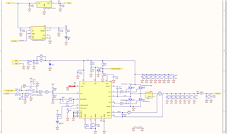
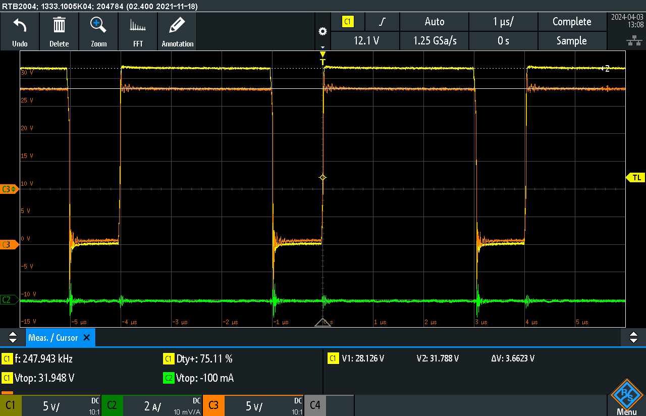
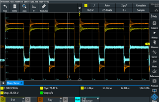
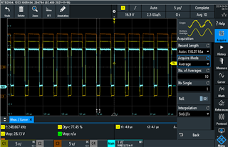
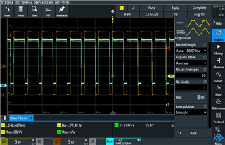
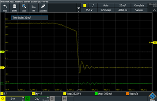
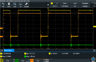
I have attached the below two pictures just to hear if anybody can confirm if these look OK. They show the switch node (SW) rising and falling edge. Input is 28V and the output is not loaded. It runs with a frequency of 250kHz.

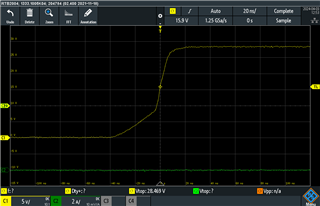
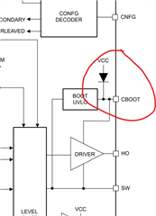
I measured the HO output togehter with the SW node. Yellow trace is HO and orange SW. I came to notice that the difference voltage is only 3.66V which seems a little low to fully turn ON the top MOSFET?

Thank you

  • Hello Thomas,

    The turn on switch looks a little slow, if using gate drive resistor, please decrease value.

    Re HO voltage levels: can you make sure the ref points are exactly the same and remeasure?  Thanks.

    David.

  • Hello David,

    There is actually a 0 ohm resistor to the gates of all the FETs. As you can see I use an external LDO to supply VCCX. This should be plenty powerfull to turn ON the FETs. Of cause it could be that two FETs in parallel is to much.

    You are correct about the ref points, I also noticed it after the previous post. I found out that on probe needed to be calibrated a bit, but after this I measured the same voltage difference. I can show a picture first thing tomorrow.

  • Sorry Thomas,

    I just realized this is the HO, out, can we measure the Vswitch node.  I think it will be fine.  Thanks.

    David.

  • Hi David,

    The first two plots is showing the switch node, rise and fall.. Do you want me to re-measure these?

    Br. Thomas

  • Hello Thomas,

    sorry for the confusion, I just checked, you are using two FETs in parallel, so will cause Tslew to be lengthen as a result of 2 x CISS of the MOSFET.

    As long as the thermal performance and efficiency meets your requirements this is OK.  If you need to increase efficiency, suggest using Low Qgtotal mosfets.

    Hope this helps.

    David.

  • Hello David,

    No problem. 

    OK so the plots of the rise fall of the switch node is as expected. I guess it will be a sweetpoint between Q_gate and Rds_on of the FETs?
    I used the calculator spreadsheet to start with.

    So far the thermals are OK, but I will properly need to cool the FETs a bit more on the next spin.

    Regarding the the plot with HO and SW, should I not expect some 5V?

    Br. Thomas

  • Hello Thomas,

    Yes, that's correct, 5V less some parasitic drops, that includes the Vf of the Boot diode as well as the drop due to the Rsouce resistance.   Make sure your probes are well calibrated.  Could try floating the scope make sure the ground of all other scope channels are not connected and use the scope channel to measure differentially across Ho and Switch.  do this or get a diff probe to measure the Ho to Switch more accurately.

    David.

  • Hello David,

    OK. I will try and measure this tomorrow.

    I can see that there is an internal diode in LM5148. The datahseet also show this on the frontpage, where an external schottky didoe is used. Could this be done?

    Br. Thomas

  • Hello Thomas,

    Yes external Diode is optional.  Thanks.

    David.

  • Hello David,

    Made two measurements, with averaging activated.

    1. Both probes floating and measured with math function

    2. Both probes measure with GND clips:

    The results are the same. I guess it is as you suggest that the internal diode drop + some additional losses are responsible for the low voltage. I will see if I can fit in a schottky diode.

    Changed the bootstrap diode from 100nF to 1uF and that helped increase the voltage to slightly over 4V. It also makes sense to me that it help as there are two FETs in parallel.

    Added a schottky from VCC to BOOT.

    Br. Thomas

  • Hello Thomas,

    Yes, the last waveforms above is ideal, when using Schottky.  

    Thanks.

    David.

  • Hello David,

    Great good to hear. The efficiency is measured to some 96.2% at 21.5V and 14.7A out.

    The only thing left is the jitter on the falling flank.

    I have per your suggestion tried to remove some capacitance, 100uF electrolytics and 20uF ceramics. Not really any impact. Have also tried to change the compensation components to have a low f_cross, but that made the transient response slow and some ringing on the output appeared. Making it faster seemed to make the jitter slightly worse.

    Br. Thomas

  • Hello Thomas,

    Depending on your layout, there is typically some jitter, how much jitter are you seeing <5% is typically acceptable.  High cross over will make jitter worse.

    I would not remove output capacitance, rather, stabilize what you have, use design calculator to ensure you are stable with enough phase margin.

    Hope this helps, 

    David.

  • Hello David,

    Thank you for the comments and suggestions.

    Cannot remember the exact numbers but think the jitter was in the low end. Will check tomorrow. 
    I think the design looks rather stable with transient and ripple.

    The layout can properly be optimized a little especially in regards of thermals.

    Br. Thomas

  • Hello David,

    Just one last question.

    When you mention layout, are there any particular parts that influence jitter more than others?

    Br. Thomas

  • Hello Thomas,

    Difficult to say exactly what is most critical in any given layout, but typically in order of priority, I would say the following.

    1. current sense feedback

    2. Power stage input caps and FET placement

    All the other recommendations will follow in priority.

    David.