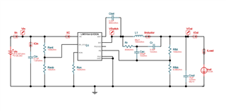
We are working on a critical design where converter stability must be a priority and, during simulations, we encountered strange behavior of the output voltage. This behavior is presented both in the Spice model (simulated in LTSpice) and in Webench. The problem does not occur in simulations on Tina TI.
Could you tell us if this behavior in the output voltage will actually occur in practice or is it some kind of problem in the simulation models?
The converter specifications are:
Input voltage: 16.5 to 40V (36V nominal);
Output current 0.2A nominal, 0.8A maximum. We designed it for 0.8A to reduce the capacitor - the simulations were run for 0.8A output current.
Output voltage: 14.5V
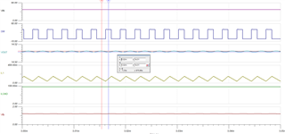
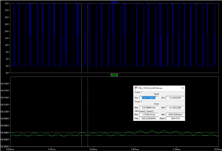
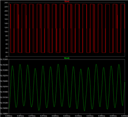
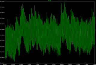
Waveforms found:
Webench:
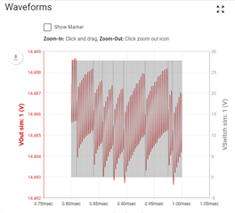
LTSpice:
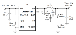
Simulated circuit:
I understand that the vertical span is small, but such variations worry us regarding the system's stability.
Thank you in advance!