This thread has been locked.
If you have a related question, please click the "Ask a related question" button in the top right corner. The newly created question will be automatically linked to this question.
Hi, Dear Appplication engineer
I'm using LM5155 to design a adjustable high voltage power supply based LM5155. the schematic as below figure shows. the input voltage is 12V. the expected output voltage is: +-5V ~+-100V. expected output current is:0.2A@+/-100V and 1.5A@+/-10V.
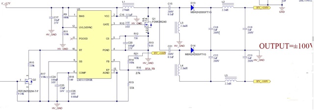
1. I can get maaximum output power is 0.17A@70.4V and 0.6A@9.5V. then the voltage will out of control and drop obviously. I can measure that drain current of MOSFET is ~2A and CS voltage is ~0.1V. the saturation current of L1 is 1.74A.
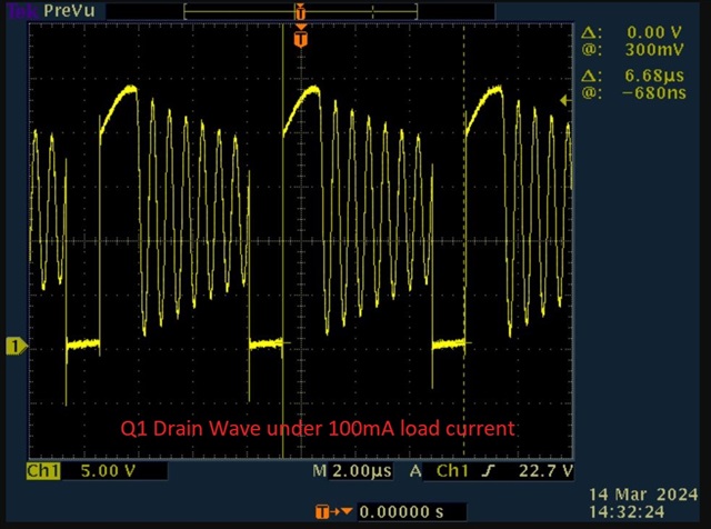
2. So, I update L1 from 270uH/1.74A to 47uH/4.4A. update L3=L4=2.2mH/0.26A to L3=L4=47uH/1.7A. update R13 from 0.05ohm to 0.01ohm. with these update, I hope the maximum output can meet my requirements. however, the maximum output will be less than 0.3A@9.5V and output will be drop and out of control.
could you please help me to calculate the compensation network value of R18, C25 and C26? remember that output will be adjusted in range of +/-5V to +/-100V.
thanks a ton for your supporting!
regards,
Bill
Hi Bill,
Thanks for using the e2e forum.
Compensating an adjustable output voltage with this large range can be rather tricky.
To build a functioning design, the compensation network must be stable for all operation conditions, including highest and lowest Vout settings.
We have a calculation tool for LM5155 SEPIC designs.
https://www.ti.com/tool/download/SNVR481
You can calculate compensation values and change the input/output parameters to check if the bode plots still show sufficient stability in different conditions.
I would recommend to start with a very slow compensation with very high phase margin.
Please let me know if there are any follow-up questions.
Best regards,
Niklas
Hi, Nikias
thank you so much for supporting!
I reviewed the excel file. in our design, we use a DAC to adjust output voltage. if we use the excel file to calculate the compensation network and fill top feedback resistor, then excel file will automatic to calculate the bottom feedback resistor that is not equal our actual value since we use a DAC to adjust output voltage. So, could I ignore the bottom resistor and just fill the bandwidth? BTW, how to select the bandwidth? thanks a ton!
regards,
Bill
Hi Bill,
Yes, you can ignore the bottom feedback resistor for your actual design and simply copy the recommended value into the excel sheet column, so the calculated bode plots becomes valid again.
For bandwidth selection, the higher the bandwidth, the faster the regulation reacts to changes, but high bandwidth normally comes at lower stability (lower phase margin).
To make the design more robust, I would recommend to go with a bandwidth lower than the recommended value to achieve higher phase margin.
In general, we recommend phase margin of 60 or more degree to have a solid design. Under worst case conditions, the phase margin might go lower.
This app note describes quite well the influence of bandwidth and phase margin:
https://www.ti.com/lit/an/slva381b/slva381b.pdf
Best regards,
Niklas