This thread has been locked.

If you have a related question, please click the "Ask a related question" button in the top right corner. The newly created question will be automatically linked to this question.

TPSM82813: schematic and placement review

Part Number: TPSM82813

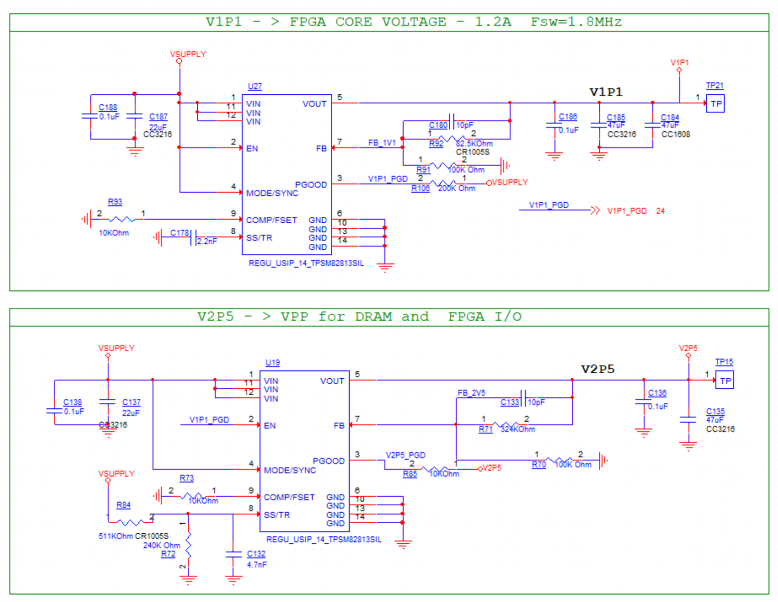
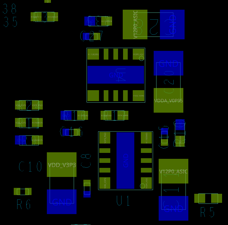
My customer is using a couple TPSM82813 right next to each other and is a bit worried about noise coupling. Can you give us your thoughts after reviewing schematics and placement? They are having them switch at different frequencies, but is that enough?

Thanks,

Brian 

  • Hello Brian,

    thanks for reaching out in E2E.

    The schematics are looking good. The resistors at COMP/FSET pin are the same for both TPSM82813, which results in the same switching frequency.

    The placement seems not to correspond to the schematics. The footprint of U1 and U4 does not match the TPSM82813 and would create a short between Vin and GND.

    Placing two TPSM82813 close next to each other has not been tested, so it is hard to say if it can be critical. The customer would have to test it.

    In general the layout of the feedback resistor divider and CFF and also the layout of the SS/TR circuitry are both critical for noise pickup and should be kept as close as possible to the FB pin and to the SS/TR pin respectively. Unfortunately the layout is not displayed in the screenshot.

    Let me know if you have further questions.

    Best regards,

    Andreas.