


Other Parts Discussed in Thread: CSD16301Q2, TPS55288, TPS552882
Hello! I am working on my own power bank application and to charge my battery (which for the purposes of assemblying was NOT connected during my tests so far), I decided to use the TPS55288-Q1 IC as a buck-boost for the typical brick chargers with PD of 5/9/15/20V down to 7.9V (for my battery).
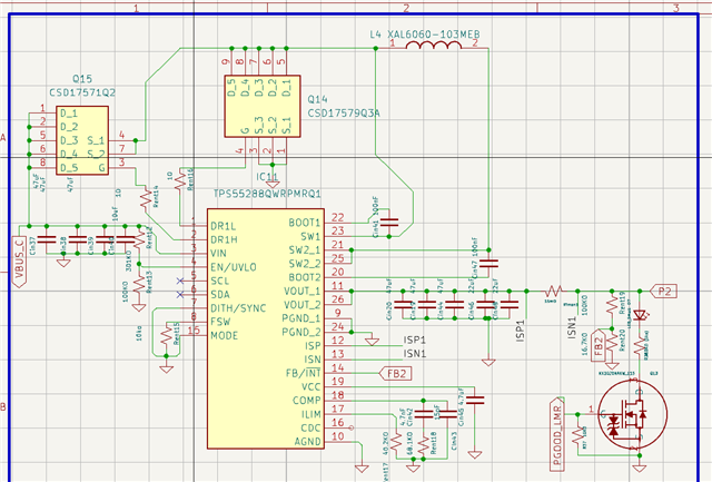
The problem is that, with almost the same components and the SAME schematic as on this webench design , it outputs only 82mV, as if nothing is even happening. I did check the input and it's indeed getting 15V from my USB PD IC. The only thing that is different is MOSFET M1, which instead of CSD17579Q3A is CSD16301Q2 which has a smaller Vgs(th) of 900mv compared to 1.1 of the latter, however it has a smaller Vgs of only +/- 8V compared to +/-20V. Could the mosfet be the problem? I mean, what even will be the voltage at its source?
One thing that sticks to my mind is the fact that WEBENCH ASSUMES 1.129V Vref for the IC, while in the datasheet at page 28 it says in the chart that 0.282V is the default voltage. I think I should've mentioned I DID NOT COMMUNICATE WITH THE IC IN ANY WAY VIA I2C. It doesn't even have a breakout on the PCB for the I2C pins. With what webench assumes, we should have: 1.129*(1+100000/16700) = 7.88V, BUT if the Vref is actually 0.282, then that would actually be 1.97V (which even so doesn't work, we're getting 82VmV).
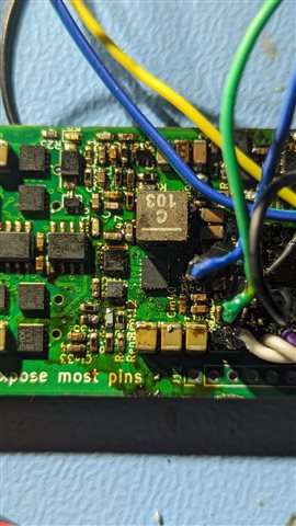
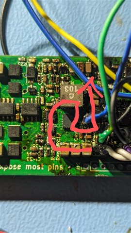
The PCB and soldered IC have no visible unwated shorts and all components were placed in the correct orrientation. I swapped 3 different TPS55288-Q1s and all of them would output about the same 80mv. Here is the kicad schematic and photos of the PCB:
What could be the problem?
