This thread has been locked.

If you have a related question, please click the "Ask a related question" button in the top right corner. The newly created question will be automatically linked to this question.

UCC28061: UCC28061: Power MOSFETs blown up

Other Parts Discussed in Thread: UCC28061

Hi,

In continuation of the previous post which I made ("UCC28061: Power MOSFETs blown up sometimes") I want to share the new measurement with you and exploring the possible issue with the MOSFETs in this design.

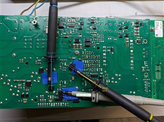
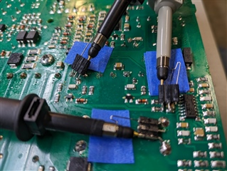
Please see the following measurements:

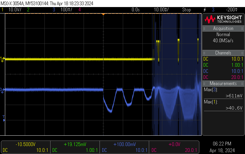
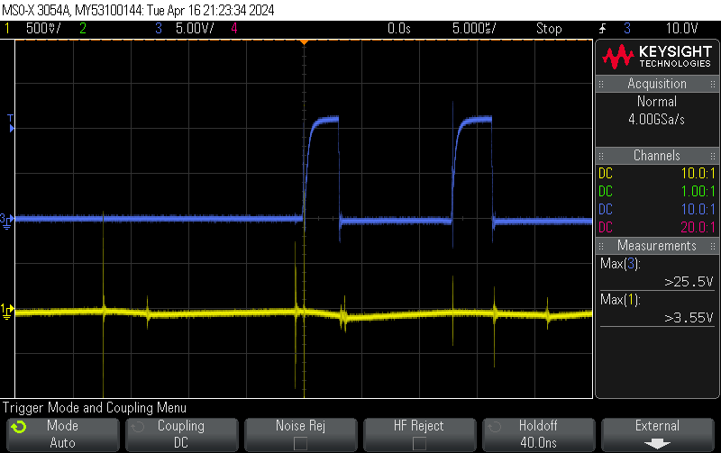
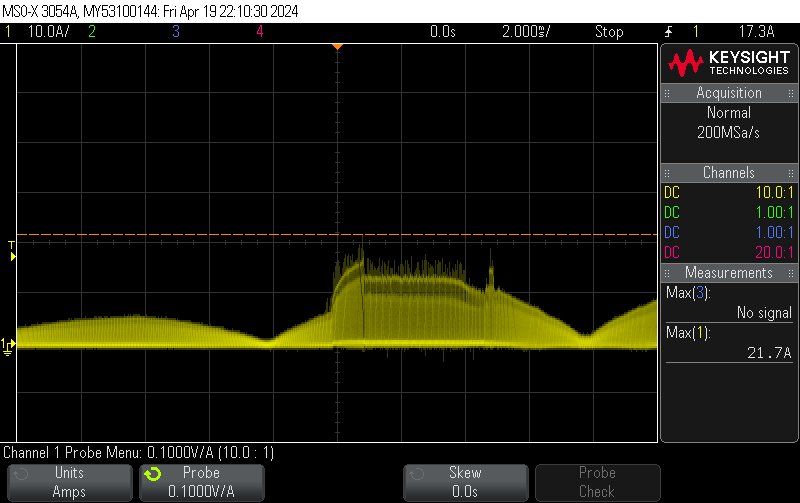
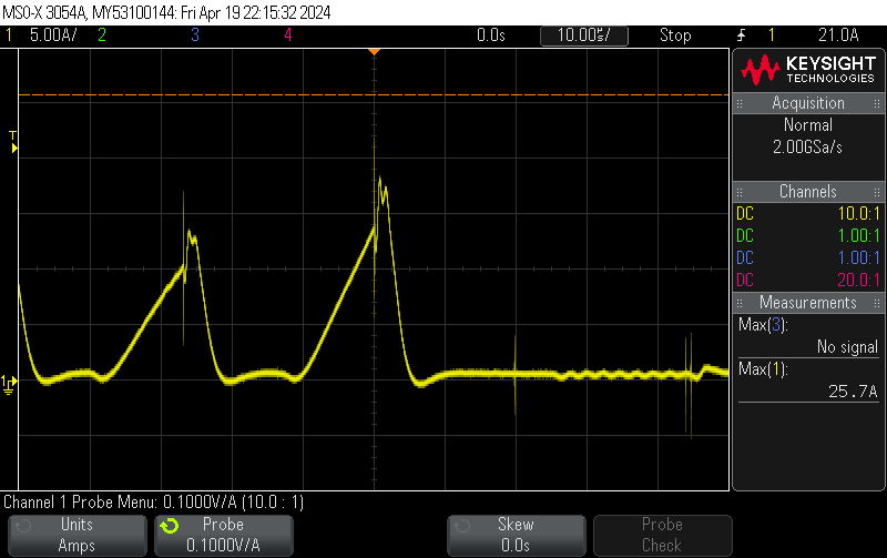
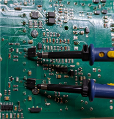
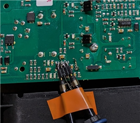
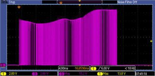
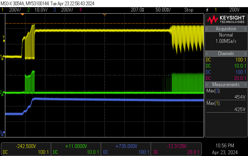
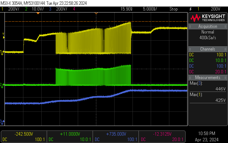
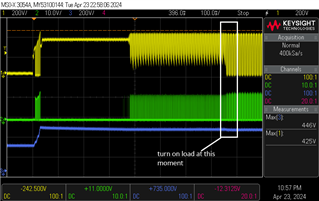
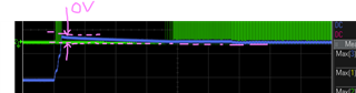
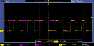
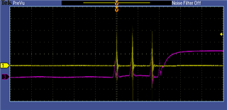
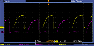
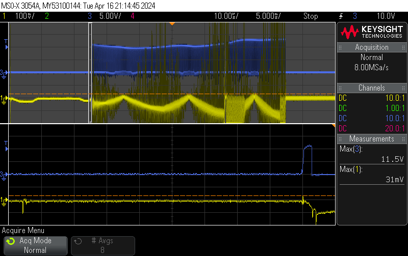
1. Measuring the GDA, GDB pins of U1 at start up (CH-1 GDA, CH-3 GDB)-Input voltage 220V AC:


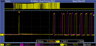
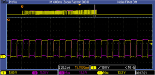
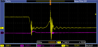
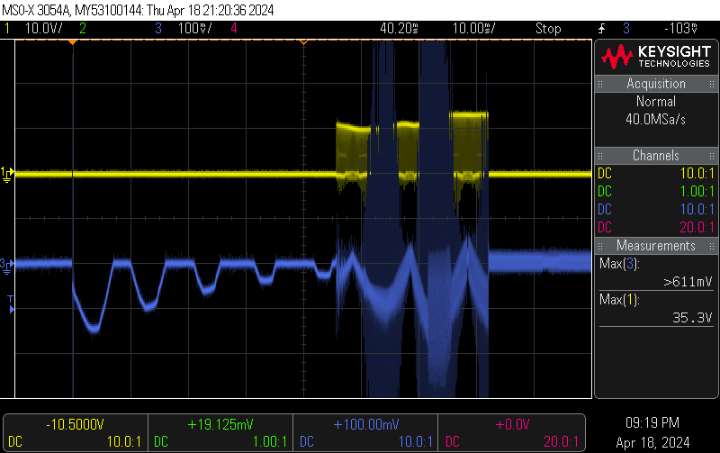
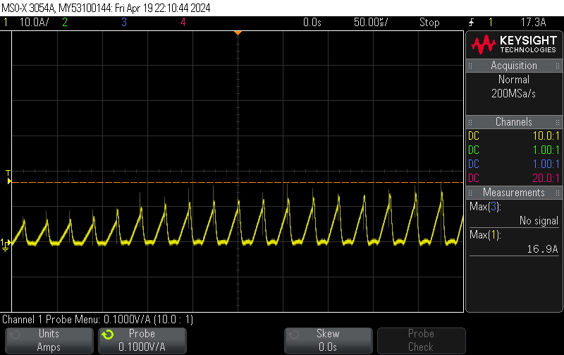
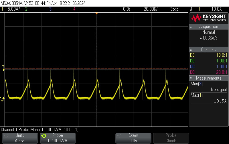
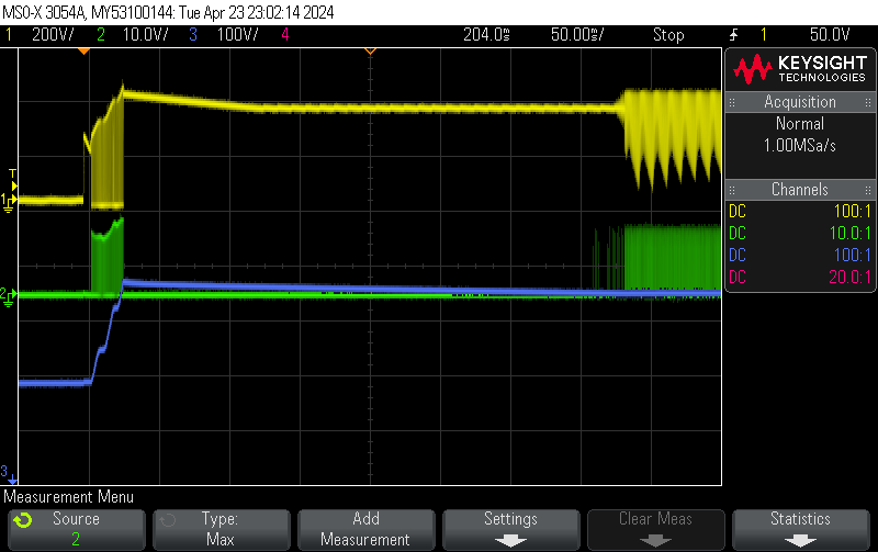
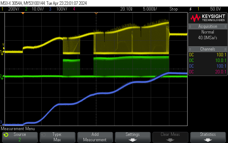
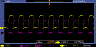
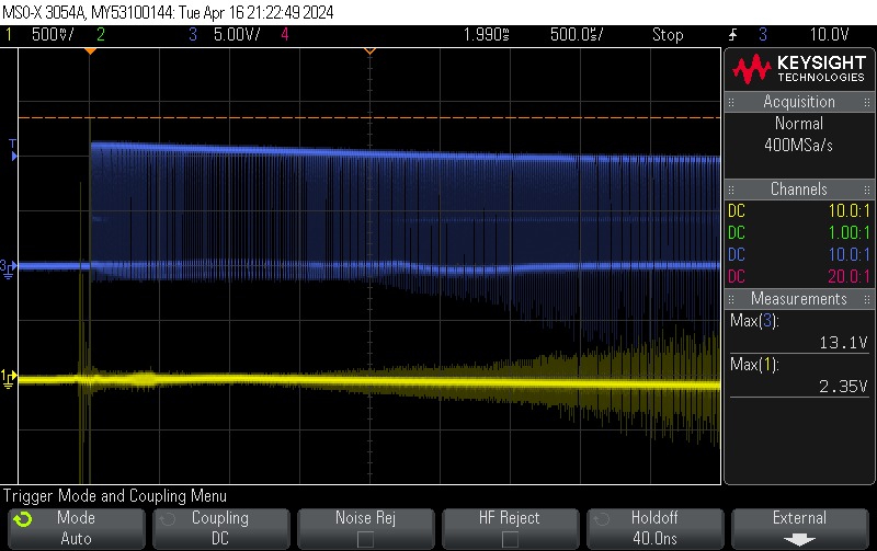
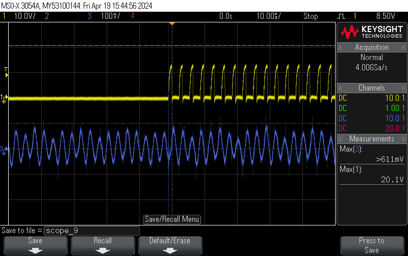
2. Measuring the GS-Q1, GS-Q3 at start up - Input voltage 220V AC:


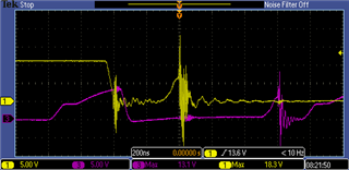
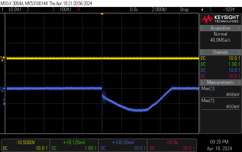
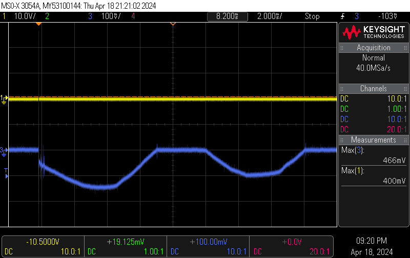
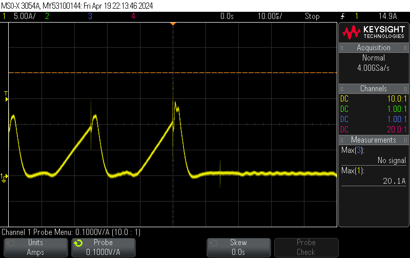
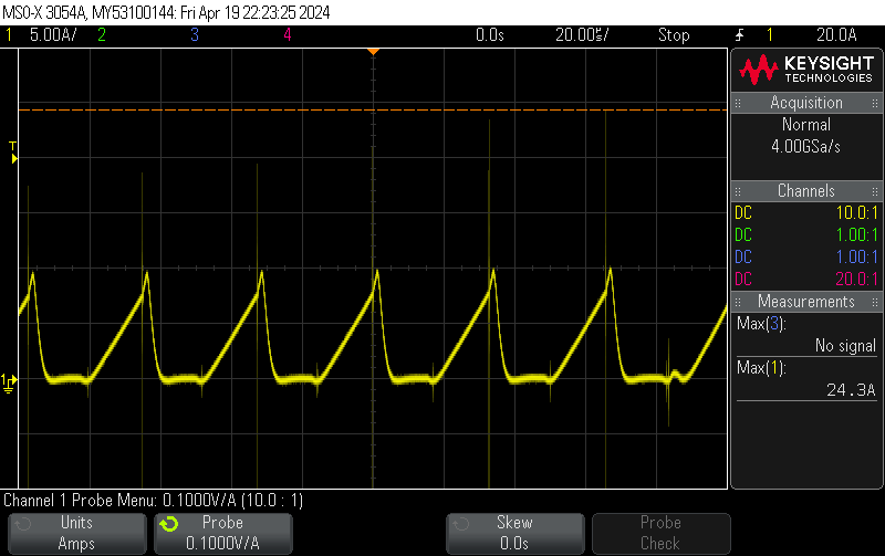
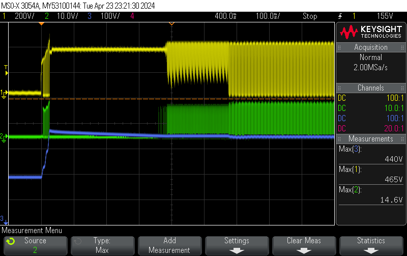
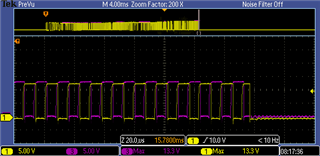
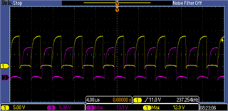
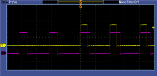
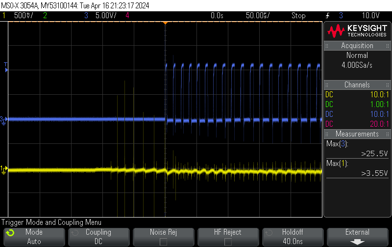
3. Measuring the GS-Q1, GS-Q3 at 200W - Input voltage 220V AC:


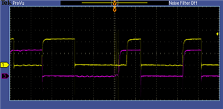
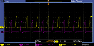
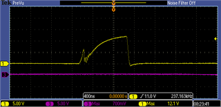
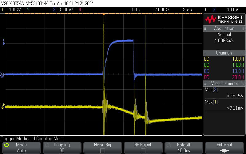
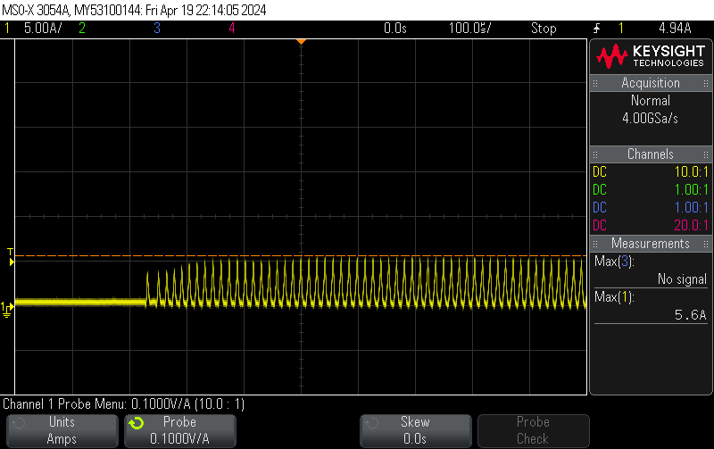
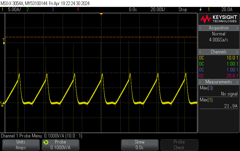
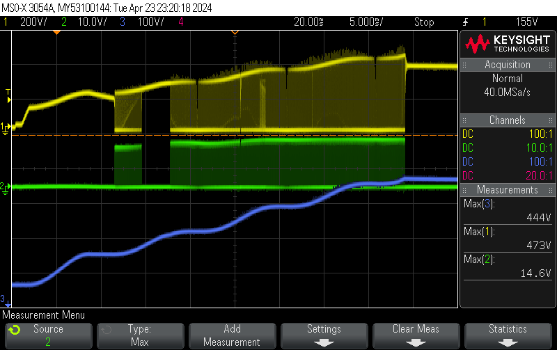
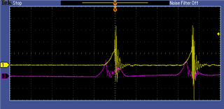
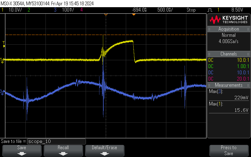
4. Measuring the GS-of CH1 at Startup - input voltage 220V, with better oscilloscope (500MHZ):


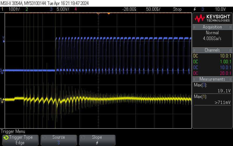
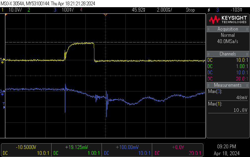
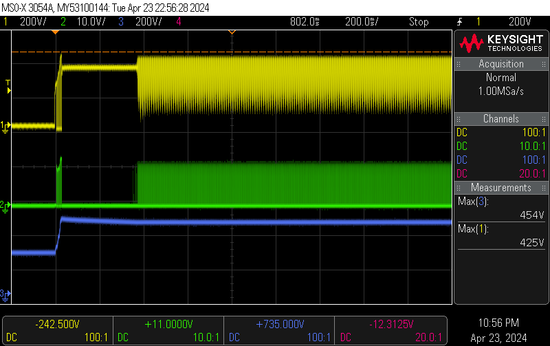
5. Measuring VCC at start-up:


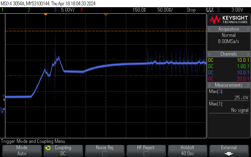
6. Measuring CS pin (U1), GS-Q1 @ 170W (CH-1: GS, CH-3: CS) - Input 220V AC:


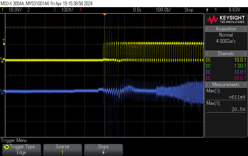
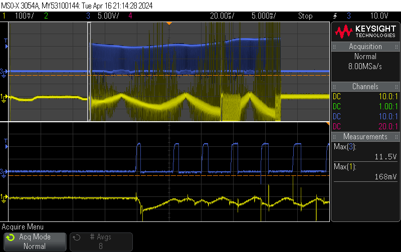
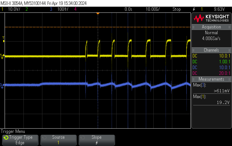
7. Measuring CS pin, GS-Q3 start up (CH-1: GS-Q3, CH-3: CS pin) - Input 220V AC:


  • 8. Measuring the DS current of the Q3 at start-up:

    Note: Please note that accurately measuring the drain-source current of the MOSFET proved challenging. I had to add a wire between the drain and the PCB to facilitate the measurement. However, each time the MOSFET blew up after approximately 5 seconds, preventing me from obtaining measurements. In the last attempt, I used a thick and as short as possible wire to measure the current. Despite conducting multiple measurements, the MOSFET blew up again after a few startups.

    See the images:

    1. Unsuccessful measurement setup:


    2. Successful measurement setup:


    The measurement results:


  • Hello Farhad, 

    I will try to help you with this issue.  I have spent some time reviewing the previous E2E thread from ~1 month ago.  

    I need to study this more but my initial suspicion is that noise may be getting into the CS input and causing unwanted restarts of the gate drive outputs. 
    Your new MOSFETs probably switch faster than the older FETs (due to lower capacitances) so faster dv/dt's may be coupling into the current sense network. 

    A PFC stage is usually followed by a DC/DC converter.  When you replaced the obsolete ST-Micro FETs in the PFC, did you also replace any MOSFETs in the down-stream converter with newer faster ones?   I wonder if switching noise from the DC/DC may also be coupling into the PFC current sense. 

    Is all of your testing above done with a resistive or E-Load, or with the actual DC/DC converter running? 

    If you reply today, I will not be able to respond until next Monday. 

    Regards,
    Ulrich

  • Hello Farhad, 

    Thank you for the additional drain current waveforms. 

    I did not see those before I posted my reply because I had the first posting open for several hours before replying. 
    Those waveforms came in while I had the first post open.

    I think the failures you get during the current probing are the result of overheating because the MOSFET has no heatsink-cooling.  
    I recommend to restore the cooling to the MOSFETs and insert the current probe in series with each boost inductor. 
    From that we can simultaneously view the inductor current, MOSFET current, and output diode current for each switching cycle.  

    The first screen capture at 2ms/div shows the current getting clipped by current limiting.  
    Can you please provide the test conditions for this waveform (input and output voltages, load power, etc.)?

    Also please provide the design targets for PFC Input and Output.
    As earlier, I won't be able to reply until next Monday, April 22.

    Regards,
    Ulrich 

  • Hi Ulrich,

    Thanks for your reply.

    As depicted in the schematic, there are two flybacks: one is dedicated to driving the module (master controller), while the other serves as the power source (utilizing UCC28061). The maximum power output is estimated to be around 600W, with a 48V output and a maximum current of 12.5A. The input voltage ranges from 85V to 265V AC, with a frequency range of 47 to 60 Hz.

    Upon connection of the PCB to the mains and activation, the master controller is energized. It then sends a signal to switch the relays (K2, followed by K1) into the on position. Subsequently, the master controller verifies the presence of the output slave devices on the line before authorizing power supply to the outputs. Therefore, immediately after startup, minimal current is drawn, resulting in a light startup.

    Therefore, I opted not to use a heat sink during startup to measure the Drain-Source current of Q3.

    Initially, I attempted to do so with a heat sink; however, accessing the power components, situated atop the PCB with large heat sinks, capacitors, and transformers, proved challenging. Consequently, I resorted to using a longer wire to connect the drain of Q3 to the PCB, allowing for attachment with a current probe. Unfortunately, the MOSFET blew up at startup, leading me to suspect that the wire I added may have contributed to the issue, and that's why as you have seen in the photos I took out the MOSFET and solder it to the Bot side of the PCB for measurement!


    Regarding your question about the MOSFETs. We only replaced the MOSFETs Q1, Q3 with a new one from ON SEMI.
    The MOSFET difference is like this:

    The left side is original (old) MOSFET from ST and the right side is the new one from ON-SEMI which has a lot of failure.

  • Hello Farhad, 

    Thank you for the background information on your system, and for confirming that only Q1 and Q3 have been changed.
    It seems to indicate that there is some aspect of the new MOSFETs that is stressed more, or rather, the old MOSFETs could handle the existing stress better. 
    We need to find out what that stress is. 

    As for the differences between the new and the old MOSFTEs, there are more differences than highlighted in your comparison chart.
    I don't think that the Pulsed Drain Current and Single-Pulse Avalanche Energy specs are the main suspects. 

    A more likely possibility is that maybe peak voltage spikes from Drain to Source due to stray inductance may be overstressing the Vds rating. 
    Since the new Fets have lower Coss above ~25V, the turn-off dI/dt may be much faster and the higher di/dt through stray inductance can generate higher voltage spikes.   I can't say this is certain, but it is worth investigating.  

    But probing must be done with the MOSFETs mounted normally on their heatsinks, and using "tip&barrel" probe technique to avoid picking up switching noise.   Similarly, Vgs can be probed with tip&barrel to verify whether there are any spikes exceeding the Vgs max rating.  

    In many of the start-up screen shots with zoom, I see that the un-zoomed part shows gate pulses for about 20~30ms and then it stops abruptly.  
    Does this happen the same way at start-up under the same conditions with the old MOSFETs?  
    Can you also please capture the PFC Vout waveform (100V/div) to see if it went into an over-voltage at 20~30ms after gate pulses started? 
    Even though an overshoot may be okay, I'd like to see if the OV goes to the same peak magnitude.  

    Regards,
    Ulrich

  • Hi Ulrich,

    The photos which have seen above were captured while I used the "Tip & Barrel" to measure the GDA, GDB, CS of U1, and GS of Q1, and GS of Q3. But anyhow, with the 500MHz oscilloscope I could be able to capture spikes (very narrow like less than 50ns). See the following images of the measuring setup:

    left photo side is measuring the GS of the MOSFETs, and right photo shows the measuring GDA, GDB pins of U1:


    During the startup phase, the GS signals are not dependent on the MOSFET type. This stage initiates system startup, transitioning it to standby mode with an output voltage of approximately 10V. The system awaits the connection of slave devices to the output line (48VPWLN-, 48VPWLN+). If these devices are detected by the master controller, the output voltage switches to 48V, enabling the system to operate normally. Subsequently, the MOSFETs adjust their switching behavior according to the load requirements.

    So the start-up initially takes around 28ms and then the system will go to standby mode and waiting for the user to turn on the load. 
    Just for your information: the slave devices are a user keypad interface and LED drivers which the user can control the light through the user interface keypad. 


    I will do the measurement to measure the PFC out (measure the C5 I guess), but I do not know what do you mean about the OV? Where should I measure exactly, I did not get that!


  • Hi Ulrich,

    I did more measurements, see the following results:

    Test setup:

    measuring the following points: 

    CH-1: DS-Q3
    CH-2: GDA-U1
    CH-3: C5

    1. Start-up (200ms/dev)


    2. Start-up (50ms/dev):


    3. Start-up + 100W load after 750ms:


    4. Start-up (5ms/dev):


    Still, I do know what is your mean about OV, please let me know to measure that.

  • Hi Farhad, 

    Thank you for the additional waveforms.  I agree, you are definitely using the tip&barrel method for probing. 

    By "OV", I do not mean "zero-volts".  It is an abbreviation for Over-Voltage. 
    What I meant was to compare the overshoots on the PFC output at start-up when using the old FETs and the new FETs, to see if there is any difference. 

    I was curious if the difference in Coss of the FETs leads to different turn-off delays (each switching cycle) which results in significantly higher or lower overshoot (over-voltage) at start-up.  I was wondering if a high OV together with high spikes from stray inductance could be overstressing the Vds of the new MOSFETs.   

    To check this, you'll have to examine the last few cycles of Vds at 5~10us/div sweep rate, and no BW limit.  This is where the OV is highest.

    Regards,
    Ulrich