This thread has been locked.

If you have a related question, please click the "Ask a related question" button in the top right corner. The newly created question will be automatically linked to this question.

LM25180-Q1: Miscellaneous questions

Part Number: LM25180-Q1
Other Parts Discussed in Thread: LM25180, , LM5180

Hello TI team,

I need to implement a PSR flyback converter using the LM25180QNGURQ1 with the following parameters:


Input voltage range:                       9-36VDC

Input threshold:                               8.5V On, 7V Off

Output voltage:                                                3.3V

Rated load current:                         0.7A

Output voltage regulation:          +/-1.5%                                               


Question 1

 Why does the WEBENCH tool lead to different component values ​​than the Excel tool?


Question 2

 The option to design a CISPR Class 5 input filter is not available in WEBENCH for this converter.  Is there an Excel tool or a TI application note available to design this filter?


Question 3

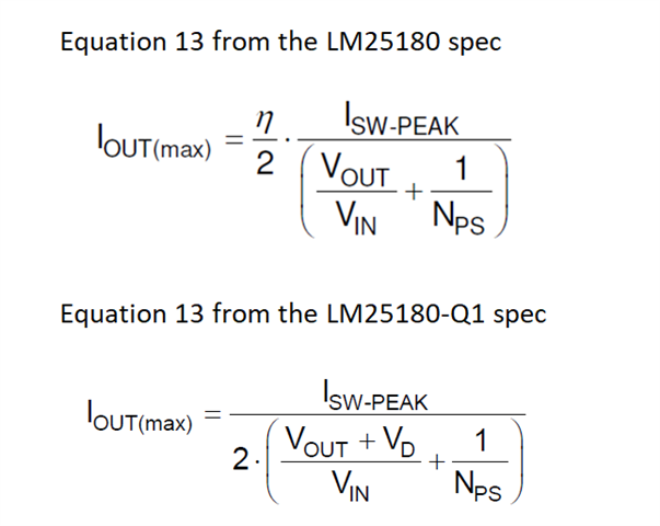
Besides being AEC-Q100 qualified, is there a difference between the LM25180 and LM25180-Q1 IC? Some of the equations used are different from one spec to the other (LM25180 vs LM25180-Q1).  As an example, equation-13 calculating Iout(max) is different from one spec to the other (LM25180 vs LM25180-Q1).  Equation 13 used in the LM25180-Q1 spec gives a result which is aligned with the Iout(max) provided in the Excel tool. Which spec equation, LM25180 or LM25180-Q1 yields more accurate results for Iout(max)?


Question 4

If the calculation of a transformer ratio leads to a ratio of 2.5:1, does it round up to 3:1 or round down to 2:1?  If the calculation gives a transformer ratio of 3:1, but this transformer is not available from any manufacturer, can you change the transformer ratio to 2:1?  The spec says that the higher the transformer ratio, the higher the stress on the SW pin of the IC.

Question 5

When calculating the flyback diode in section 8.2.1.2.4, it says “In general, choose a flyback diode with current rating greater than the maximum peak secondary winding current of NPS*IPRI-PK(max)”.  For my design, it gives 3x1.5A = 4.5A minimum.  Can this current be multiplied by the maximum Duty Cycle factor to lower this current? Indeed, it seems that this current is not continuous at maximum Duty Cycle or short circuit.  The maximum DC for this design is around 60% at Vin(min), which gives: 0.6x3x1.5A = 2.7A for maximum diode current.  To support this affirmation, WEBENCH recommends a flyback diode of 3A for this design.  The example given is section 8.2.1.2.4, also lowers the diode current with the maximum Duty Cycle.


Question 6

Can Low ESR Tantalum capacitors be used for Cout?  For some reason, I cannot find any 100uF/6.3V MLCC with soft/flexible terminations.  The environment for this design is automotive therefore SMD ceramic capacitors with soft terminations are a must. I do realize that the Capacitor ESR will interfere with the poles of the control loop.

Question 7

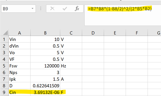
How do you get the result of 2uF for Cin using equation 24 in the example design of section 8.2.1.2.7?  No matter how I calculate, I always get 0.35uF as a result.  I used equation 4 for IPRI-PK(BCM) to calculate the current.


Question 8

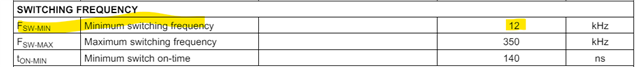
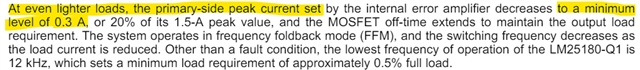
Is there an equation to determine the minimum load required?  In the past, I have used the following formula with PSR flyback from other manufacturers: “Lpri x [ISW-PEAK(FFM)] x f(min)/ 2xVout” which leads to around 5mA.  LM25180-Q1 spec section 7.3.2 says “Other than a fault condition, the lowest frequency of operation of the LM25180-Q1 is 12KHz, which sets a minimum load requirement of approximately 0.5% full load” gives 0.005x0.88A = 4.4mA.  WEBENCH recommends 4.1mA.  Which minimum current is correct?


Thank you,


Regards


Eric...


  • Hi Eric,

    Thank you for posting. There are lot of questions.  Please allow me sometime and I should get back to you in the next couple of days.

    Thanks,

    Youhao

  • Hi Eric,

    Sorry for the delay.  Here are answers to your questions.

    A1.  The Webench model is based on our EVM and some tradeoffs in deciding a component selection is less flexible than using the design calculator.  Note that either one is intended to get you to a good start point, and it is always needed to fine tune the design after experiments.  To choose between, I would prefer the calculator, for it gives you more control in tailor the design.

    A2. EMI is usually considered a system level issue, and the LM5180 circuit may just be a small part of your overall system. Please refer to the following seminar regarding EMI. https://www.ti.com/lit/pdf/slyp757?keyMatch=emi%20filter%20design

    A3. The equation with the efficiency parameter included is more accurate.  The two devices (-Q and non-Q versions) are basically the same by IC design.

    A4. Sorry our calculator just includes limited number of turns-ratio options, mainly due to more complexity in the background calculation it could bring by finer granulation of the turns ration options.  Yes you can either round up or down to choose an available number in the pull-down menu, but double check the peak current at the min Vin and also the max duty cycle, as well as the min inductance suggested by the calculator, to make sure the roundup is okay.

    A5.  Datasheet recommendation is a good practice and conservative, but yes you can scale it down by applying the duty cycle, but note that here it should be (1-Dmin) for the diode.  Whatever, you should make sure the selected diode has a physical size able to handle the heat under full-load. 

    A6. Yes you can use Tantalum. 

    A7.  Allow me some time to take a look and get back to you later.

    A8. The typical min load can be estimates as:  0.5 x Lmag x 0.3A^2 *12kHz.   It is because the peak current will always be at 0.3A, and switched at 12kHz. 

    Thanks,

    Youhao

  • Hi Youhao,

    Thanks for your answers.

    Regarding A3.

    Is there a formula to calculate the efficiency?  All I have are the graphics from the Calculator and Webench, that don't seem to compare.

    (Calculator)

    (Webench)

    Regarding A6.

    The lower the ESR, the lower the voltage ripple at Cout but is there a min/max ESR value that should be respected for loop stability?

    I know that the ESR value for the ceramic capacitor is quite low compared to the tantalum capacitor.

    Regarding A7.

    Thanks. I will wait for your answer.

    Regarding A8.

    Your formula gives 16.2mA of load, which is too high.

    Please let me reformulate my question A8.  Is there a minimum load that needs to be provided on Vout to insure stability of the converter?

    How do you calculate this minimum load required?


    Thank you

    Eric   

  • Hi Eric,

    Sorry for some typos during editing.  I re-edited this reply. Sorry for the confusion.

    ---------------------

    Those are good questions.  Let me try to clarify.

    All calculated efficiencies are basically an estimate.  Since the Webench is limited largely to the EVM design, I would take the calculator efficiency prediction as the estimate. The efficiency calculation is rather complex but you may refer to the following articles in which some power dissipation calculation equations can be used.  

    https://www.ti.com/lit/pdf/snva805

    https://www.ti.com/document-viewer/lit/html/ssztcy0?keyMatch=flyback%20converter%20design

    https://www.ti.com/document-viewer/lit/html/ssztcw6?keyMatch=flyback%20converter%20design

    Regarding A6,  the big ESR would affect the loop because the loop compensation is internally fixed. The internal compensation is not disclosed but as long as you follow the design equations given in the datasheet, or follow the design calculator to keep ripple voltage below 1%, then it will be okay. 

    Regarding A8, the circuit would be stable but Vout can shoots up if min load conditions does not meet. 16.2mA is less than 2% of your full load, why do you say it is "too high"?  You may use a Zener diode of about 5 to 10% above your Vout setting voltage, instead of using a dummy load resistor, then you can avoid permanent power loss at higher load. 

    Regarding A7, I am waiting for my mathcad to work on my new laptop.  I will update ASAP.

    Good luck in your project.

    Thanks,

    Youhao

  • Hi Youhao,

    Thanks for your answers and patience.

    Regarding A3.

    I will take the efficiency value from the calculator (80%). Thanks

    Regarding A6.

    I just looked at the tantalum capacitor spec.  Even the capacitor series recommended for power supply cannot

    give me an ESR that gives me a voltage ripple under 33mV (1% of 3.3V).  My application is at 105C and there are

    a lot of deratings to be applied with temperature for these capacitors (Irms(max) current).

    Can I parallel the capacitors ESR to lower the total? No wonder the spec advises to use ceramic caps.

    Regarding A8.

    I mean 16.2mA is high compared to the dummy load from the calculator (5mA) and WEBENCH (3.3V/806ohm = 4.1mA),

    It is like 4x higher.

    Thank you

    Eric 

  • Hi Eric,

    Regarding A6, yes you can parallel capacitors and it is actually the way to lower the total effective ESR.

    Regarding A8, what is your transformer inductance?

    Regarding A7, sorry I am still struggling with my new laptop to make Mathcad work...  

    Thanks,

    Youhao

  • Hi Youhao,

    Regarding A5

    You mean (1-Dmax)? IPRI-PK (and RMS) current are higher at Vin(min).  When calculating at (1-Dmin) @36V

    the currents are lower. 

    Regarding A8

    For a double footprint on the PCB,

    Xfo#1 --> Wurth P/N 750313974, 40uH, turns ratio 3:1:1, 2A

    Xfo#2 --> Coilcraft P/N YA8779-BLD, 30uH, turns ratio 3:1:1, 2A

    Thanks 

    Eric...

  • Hi Eric,

    Regarding A5, (1-Dmax) can be another way, but if want to be more conservative, take the worst case for the diode, assuming the current flows longer time.  The actually power dissipation is always VF * Io, but VF can be higher when your off time is shorter.  Using the quick guide in the datasheet namely 3x Isec pk would not be safer. 

    I use 40uH and the calculated dummy load is 6.5mA.  How could you get 16.2mA?

    P_dummy = 0.5 * 40uH *0.3A^2 * 12kHz = 0.5*0.00004*0.3^2*12000 = 21.6W

    I_dummy = P_dummy / Vout = 21.6mW / 3.3V = 6.5mA.

    Using the 30uH would have lower dummy load current. 

    Could you recheck your calculation?

    Thanks,

    Youhao

  • Hi Youhao,

    Understood for A5

    Regarding A7

    Let me know when you'll be able to do the calculation for Cin. 

    Regarding A8

    You are right. I think there is a confusion, from my part, between "mA" and "mW" that comes from the initial equation.

    The first formula divided by Vout which gave the minimum load current directly.

    Your calculation gives the result in mW (16.2mW for 30uH/21.6mW for 40uH).

    Thanks for pointing that out. So "Rdummy = 0.5 x Lmag x 0.3A^2 *12kHz/3.3V".

    Thanks

    Eric

  • Hi Eric,

    I have been struggling to get my mathcad work on this new laptop, but I change to hand calculation in order not to further delay your work.  This is what  I found: Equation (24) of the datasheet for Cin calculation is corrected. It is based on charging and discharging of Cin by the input current.  Consider the datasheet example design, the frequency at 10Vin would be ~120kHz (refer to design calculator), then the equation gives a result of 3.69uF.  My hand writing was messy, so I re-captured the calculation in Excel. Note that Duty cycle D is calculated by (Vo + VF) / (Vo + VF +Vin/Nps)

    Hope this clarifies. 

    Best Regards,

    Youhao

  • Hi Youhao,

    It's not fun when your tools are not working.

    The result of 3.69uF makes more sense. I recalculated the Cin for my design at Vin(min) = 7V.

    Using a calculated D = 0.61 and IPRI-PK = 1.2A. Fixing FSW ~= 120KHz.

    Cin(min) = 5.26uF (Using equation 24 with ISW-Peak = 1.5A)

    Cin(min) = 4.21uF (Using equation 24 with IPRI-PK = 1.2A)


    Thank you and have a nice week end

    Eric...