


Other Parts Discussed in Thread: UCC21750
A month ago, I started a thread here, describing the issue I was having with the IC. After a while and 20 hours of testing where everything was ok, The IC´s VCC and VEE pins got damaged without any apparent reason and were shortcircuited.
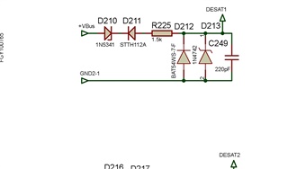
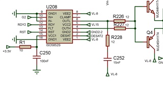
The IC ISO5852S was used as part of two driver circuit for a half-bridge LLC resonant converter. One driver was responsible for triggering two switches ( Working in parallel to divide the current on the switches) at the upper part of the leg of the half-bridge, and the other one is responsible for triggering two switches ( again, working in parallel to divide the current on the switches) at the lower part of the leg.
The operational details of the circuit are:
-The switching frequency of the converter was 80 kHz.
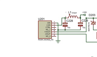
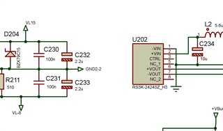
-The power side of the ICs was supplied by a DC-DC isolated converter RS3K-2424SZ (24 V output and 3W).
-The power of the half-bridge converter is 6 kW.
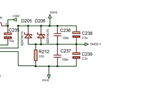
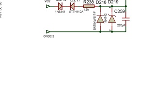
Again, for a better understanding of the design, below the schematic of the circuit is depicted.
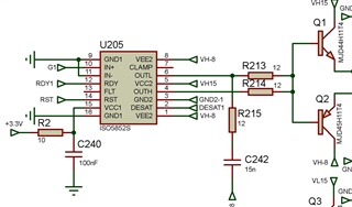
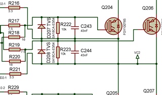
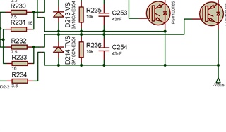
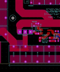
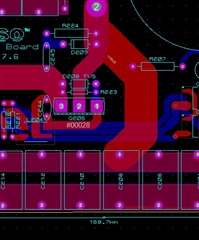
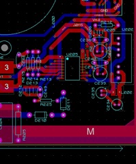
For a better idea of how the layout was designed, below is a depicted part of it, showing the circuitry related to the Gate Drive responsible for the switches on the upper side of the inverter.
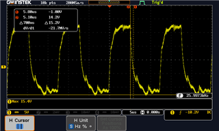
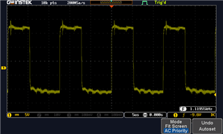
The gate waveform of the four switches is depicted below.
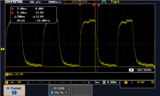
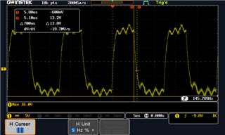
Lower Switches:
a
The waveform on the output of each IC is also depicted below. In the first thread here, I was asked to send this waveform, but because at that point we thought the issue was already solved, I completely forgot to send it.
First IC:
OUTH OUTL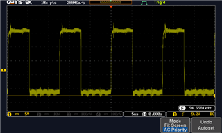
Second IC:
OUTH OUTL
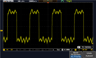
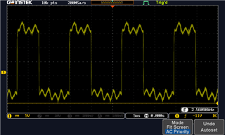
All waveforms presented here were saved when the equipment was operating at full power, in our laboratory.
At the moment of failure, our equipment was already with 20 hours of testing. the room temperature around the metal case where the PCB was inside, was around 50 degrees Celsius.
We didn´t measure the room temperature inside the case, but we estimate that it should be around 60 degrees Celsius or even more.
Our equipment operates on the field under harsh conditions. It is carried on the back of a tractor, inside a metal case that stays under the sun for hours, while it is on.
Do you have any idea of what might be happening with the IC?
In the worst case, just for a matter of testing, is there any other IC that is more robust and can replace this one?
Obs: In order to solve the noise issues presented in the waveforms above, a new layout design was already made, but we still don´t have the PCBs yet.
