This thread has been locked.

If you have a related question, please click the "Ask a related question" button in the top right corner. The newly created question will be automatically linked to this question.

LMR33640: LMR33640ADDAR output +5V/4A and the other LMR33640ADDAR is as inverting buck-boot to generate -5A/2A from 12V/2A

Part Number: LMR33640
Other Parts Discussed in Thread: LMR33630

Hi Ti,

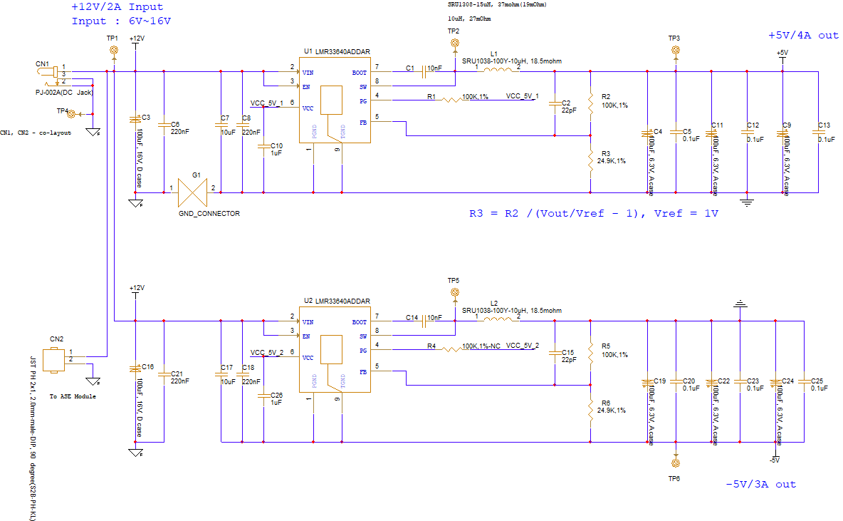
Pleaase help review below schematics, one LMR33640ADDAR output +5V/4A(3A is OK) and the other LMR33640ADDAR is as inverting buck-boot to generate -5A/2A from 12V/2A

Please  you recommend changes in the design, thanks

  • Hi Jerry,

    Thank you for sending your schematics, here are my comments:

    1. This device is designed with a 100 nF CBOOT capacitor in mind. C1 and C14 should both be 100 nF ceramic capacitors.
    2. For a 5 V output, TI would recommend at least 10 V of voltage rating on COUT (16 V to be safe). 6.3 V rated capacitors will likely de-rate significantly under a 5 V output and not provide sufficient capacitance.
    3. The same for output can be said for input. TI recommends at least 25 - 50 V of voltage rating on CIN as 12 V input voltages would cause significant de-rating on 16 V rated capacitors.
    4. Ensure your inductor saturation current ratings are at least as high as the high-side switch current limit (6.2 A). For an inverting buck boost a higher current rating may be required. You can check the new current stresses with equations 4 and 5 in this app note.
    5. PGOOD requires a level shifter to be effective in an inverting buck boost (IBB) application due to the relocation of the GND reference in the IC. Section 7.3 in the same app note can help idealize the required level shifter for PGOOD.
    6. A minimum of 10 uF of ceramic input capacitance is required for the IBB circuit. C17 and C18 become the "bypass" capacitance for the device in an IBB configuration. I believe C16 is an electrolytic? If this is the case, an extra 10 uF ceramic capacitor with 50 V of rating from VIN to GND (not IC GND) should be used on input for the U2 circuit.

    Hope this helps and please let me know if you have any questions,

    Joshua Austria

  • Hi Joshua,

    Thanks for the schematics review and suggestions

    About PGOOD in the buck down and inverting buck boost, actually my application does not need PGOOD signal to reset the system, Does it mean that Ican leave the PGOOD pin as no connection?

    About C17(10uF) and C18(220nF), according to your suggestions, can I move the GND (IC GND) of C17(10uF) to input GND?

  • Hi Jerry,

    Yes, you can leave PGOOD floating if not using it. 

    In terms of C17, you will still need a 10 uF capacitor from VIN to IC GND. Although this capacitor is no longer providing input capacitance it is still supplying ripple current and isolating the board switching noise from the internal control circuits. It is recommended that C17 and C18 remain where they are in your schematic.

    For this part, as the datasheet requires ceramics on input, you will still need to add an extra ceramic of 10 uF from input to system ground in parallel with C16. 

    Thank you,
    Joshua Austria

  • Hi Joshua,

    Thanks for your very clean suggestions.

    Another question, it looks that LMR33630ADDAR is pin to pin compatible with LMR33640ADDAR .

    Whether I can replace LMR33640ADDAR with LMR33630ADDAR  in this schematic design and install LMR33630ADDAR to the PCB which was desiged for LMR33640ADDAR directly ?

  • Hi Jerry,

    Yes, as the two devices are pin to pin compatible, you can use the LMR33630 to replace the LMR33640. Keep in mind however that the current limit is a little lower (3 A as opposed to 4 A) and that in an inverting buck boost configuration, this current may be more limited. For more information you can check the app note on inverting buck-boost configurations that was shared before.

    Thank you,

    Joshua Austria