This thread has been locked.
If you have a related question, please click the "Ask a related question" button in the top right corner. The newly created question will be automatically linked to this question.
Hi,
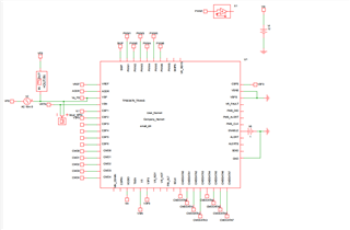
I want to used part no:- TPS53679 for our new design to provide power for Intel Xeon Processor D-1746TER (Idaville).
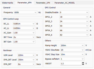
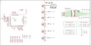
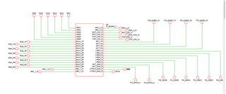
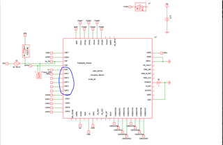
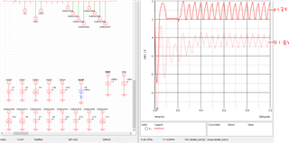
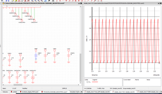
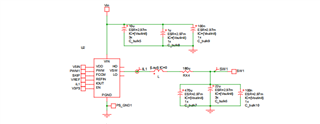
we found SIMPLIS model of part no:-TPS53679 from TI. and when we simulate this model using simplis tools we are getting output result attached image below, but i am not sure about the output reslut wheater is it correct or not. can you please suggest is it correct or not.?
we want to use this model for output 1.2V but we are getting output variation from 1V to 1.8V. what type of output waveform we can see.? can you please suggest any reference simulation result of part no TPS53679?
can we program/change output voltage and how we will do please suggest ?
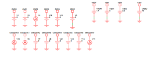
for your reference we have attached simulation result and simulation schematic image of TPS53679
Thanks
Niranjan
Hi Niranjan,
I see that Lout(inductance) value is not mentioned in the attached images. Please check that L value is assigned in schematic.
The Vout waveform is not expected. Can you tell us the what are these parameters set to , as shown in below picture. You will get a dialog box on double clicking the TPS53679 simplis model.
1) You can use the Vboot value to change the output voltage.
2) Please verify that the output capacitance that you are using in the schematic is matching with the design value.
3) Please be sure that the parasitics are matching with the original design.
Best Regards,
Chanakya.
Hi Chanakya
I have done above setting in my simulation. But we have one dought regarding TPS53679 output,
1.) which point we need to probe to get the correct out put? For your reference we have marked two point attached below image.
2.)What is U8? and why used in below schematic
3.)As we are going to use only one phase among these 6 phases. other 5 phases to be disabled by connecting CSP2 to 3P3 supply. While doing so, where do we have to keep the probe?
We have tried to probe at SW1 position but results were not satisfactory, please refer to previous post for attached output waveforms
Thanks
Niranjan
Hi Niranjan,
1) Please probe on the VSP pin of corresponding rail, which is the actual output going as feedback to controller.
2) This block is used to connect the output bulk capacitors , output load to power stages. The corresponding labels on this block will let you know the corresponding connections on schematic.
3) Yes, you can probe at SW1.
Please check that the bulk capacitor value in schematic and the designed value are matching along with parasitic values.
Best Regards,
Chanakya.