This thread has been locked.

If you have a related question, please click the "Ask a related question" button in the top right corner. The newly created question will be automatically linked to this question.

TPS55288: MOSFET damaged issue

Part Number: TPS55288

Hi,

We have occur TPS55288 MOSFET damaged issue, would you please add me friend?

I will pass schematic and layout for you reveiw to check if any possible to cause this issue. thanks!

Jeff

  • Hi Jeff,

    You can send the schematic and layout files to me via private message.

    May I know what is the application and the input/output operation conditions?

    BRs,

    Bryce

  • Hi Bryce,

    I've send it to you.

    And may I know the DR1H/DR1L 1ohm resistor is recommend for normal design?I found it on EVM.

    It should for reduce gate driver EMI noise purpose?

    Thanks!

    Jeff

  • Hi Jeff,

    1. I can't open the .pcb file, can you share the screenshots of each layout of TPS55288 part?

    2. On the customer board, only Buck side MOSFET are damaged? What about the IC itself?

    3. Can the customer show the waveforms of DR1L, DR1H, SW1? 

    4. What is the input voltage range, output voltage range and max output current?

    5. What is the part number of the output capacitors(C668-C670, EC16)?

    6. Yes, the gate resistor is used to slow the driver speed and reduce the noise, recommend to change it to 0ohm.

    BRs,

    Bryce

  • Hi Bryce,

    1. I can't open the .pcb file, can you share the screenshots of each layout of TPS55288 part?

    => ok, will provide it later.

    2. On the customer board, only Buck side MOSFET are damaged? What about the IC itself?

    =>Yes, only buck high side damaged. IC are fine.

    3. Can the customer show the waveforms of DR1L, DR1H, SW1?

    => ok, will provide it later.

    4. What is the input voltage range, output voltage range and max output current?

    => ok, will provide it later.

    5. What is the part number of the output capacitors(C668-C670, EC16)?

    => ok, will provide it later.

    6. Yes, the gate resistor is used to slow the driver speed and reduce the noise, recommend to change it to 0ohm.

  • Hi Jeff,

    Thanks for the files and waveforms. 

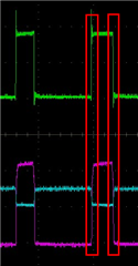
    What is the failure rate of the MOSFET damage? Can the customer probe the waveforms of DR1H, DR1L and SW1 at the time of failure? 

    And can they zoom in the waveform in 5ns/div?

    About the schematic:

    1. For the EC16, I don't find the datasheet online, can you share this with me so I can check the COMP parameters. Or the customer can also check the phase margin by observing the output voltage ripple during load transient as below note mentioned.

    https://www.ti.com/lit/pdf/slva381

    2. Recommend to change R538=R537=0ohm;

    3. What is the input voltage range, output voltage range and max output current? Recommend to set lower average inductor current limit with higher value of R555.

    4. I also don't find the information of L45, what is saturation current for this? Recommend to select the inductor with saturation current > average inductor current limit value.

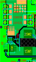
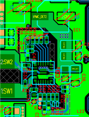
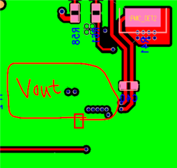
    About the layout, it look poor especially with the relief connection of GND connections which would introduce large parasitic parameters into the power loop and cause higher voltage spike.

    1. Use solid connections for all GND connections.

    2. Add the 0.1uF/0402 ceramic capacitor close to Vin and GND net.

    3. Add one 0.1uF/0402 output ceramic capacitor more close to Vout and GND pins. And use solid connection for GND connection.

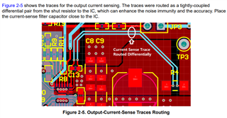
    4. Use Kelvin connection for ISP and ISN connections.

    5. Recommend to add one more 0.1uF/0402 ceramic capacitor close to Vout vias and GND plane at the bottom layer.

    BRs,

    Bryce

  • Hi Jeff,

    Thank you for confirmation that the issue is caused by the Q1 gate pin soldering issue. I will close this thread now, please also follow the sch and layout recommendation as replied above.

    BRs,

    Bryce