This thread has been locked.

If you have a related question, please click the "Ask a related question" button in the top right corner. The newly created question will be automatically linked to this question.

TPS92643-Q1: UDIM under voltage

Part Number: TPS92643-Q1

Hi team,

My customer wants to use TPS92643-Q1 for a constant current drive design of the solenoid valve and has the following questions:

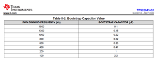
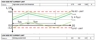
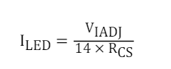
Q1: How can I merely use UDIM as under-voltage lockout ? In the specification, this port is multifunctional can set VUDIM and Under voltage Lockout. However the threshold voltage of VUDIM is two times larger than Under-voltage Lockout . When it comes to operation voltage, it's very difficult to set an appropriate under-voltage threshold voltage to make the chip work and active the error amplifier and COMP compensation.

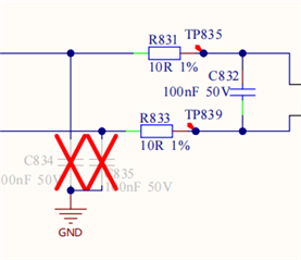
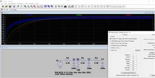
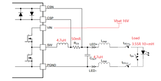
Q2: The below picture shows how we want to use UDIM, APWM, and IADJ. We want to set UDIM as under voltage lockout also controlled by MCU to actively cut the ship off , APWM as Enable with 100% duty pwm to enable or disable the ship, and IADJ as the current modulation by timely input different voltage . Here is my question, if I disable the chip or totally shut down it, would there be some logical problem like firstly pull down IADJ , then the APWM , finally the UDIM, wouldn't it?

Thanks!

Regards,

Ivy

  • Hello Ivy,

    Q1:  I agree, the Drop Out feature of the part isn't really useful and can cause problems.  Unfortunately, I didn't make the decision for that feature and we have to live with it.  The intent of the feature was to be able to drive an LED during cold crank, but making the drop out threshold 2x the UVLO threshold is problematic.  It should have been much closer to the UVLO threshold to make it useful.  

    Q2:  IADJ, APWM, and UDIM are all logic anded together so is any of them are pulled low it will shut off the output and it won't turn on until all the signals are high.  It doesn't matter the order.  

    Let me know if this isn't clear.  

    -fhoude

  • Hi fhoude,

    I'm the one who ask for upper problem. Here comes more question:

    Q3:The bootstrap capacitor value is recommended in the specification changed with PWM dimming frequency. How should I understand the PWM dimming? the frequency type I know is the Fsw. In the design , we plan to use the APWM as 100% duty all the time ,so there won't be any duty change.

    Q4: As I searched, noted the bootstrap capacitor is related to the leakage current of DIODE ,MOSFET ,BOOTSTRAP CAPACITOR,BOOTSTRAP CIRCUIT,   and BOOTSTRAP QUIESCENT . Is that resistor should be counted in or the resistor should also be changed with different capacitor ? 

  • Q3:  If you aren't doing PWM dimming then you don't have to oversize your bootstrap capacitor such that it stays charged during the Off Time of the PWM signal.  You can use 0.1uF or something like that.  

    Q4.  Most of the leakage is from inside the device.  If you look at our tables in the datasheet we give recommended values for bootstrap capacitor for various PWM frequencies.  This table takes into account the leakage from our part.

  • I‘m very pleased get so complete and detialed answers !

    OKAY, I'll place a 0.1uF capacitor at here.

    Thank you !

  • Hi Fhoude,

         Sorry to bother you again.I have two more questions on using the ship.

          Q5:Do you recommend place the RC filter  in the CSP and CSN pin for percisely collecting current?  And what value of the capacitance and resistor you suggest? Show in P1.

          Q6:The VADJ pin is used for current modulation. Normally, I use the DAC function,but the MCU I use don't have it. If I adopt the three level RC to make PWM into a stable voltage,what about the voltage difference the ship required,  is the 5mV fit or larger ? Show in P2.

    P1. CSP CSN filter

    P2. three level RC

  • Hello K SX,

    P1.  Putting an RC filter on CSP and CSN is usually not very effective and not needed.  Keep in mind that the current sense resistor is ~50 mOhms.  In order to effectively filter any noise it would have to be a huge capacitor as you don't want a large series resistor with CSN and CSP signals.  We generally don't use it.  We also have blanking period to ignore high frequency current noise during the turn on and off transitions of the synchronous FETs.  

    P2.  Yes, you can low pass filter a PWM signal to control the voltage on IADJ pin.  You will have to choose components appropriately and verify accuracy.  

    -fhoude

  • Yeah, the current sense resistor is 50mR. According to the specification, I=V/(14*0.05) , like 0.01A equals to 7mV. I mean ,the ripple voltage is no larger than 2mV , does the IADJ has such percision can realize the 2mV difference? Can you tell me its percision if you have such information?

  • Hi Fhoude,

             I have a serious issue about this ship. 

             For the Isink(LS), the specification tells me it's 2A @min (from Drain to PGND).

            Q7:Here comes to an problem , the Isink limitation is from Drain to PGND(short as DTP) , is there have current limitation from PGND to Drain(short as PTD) ? Or the limititation PTD equals to the Isource at the high-side.

           Q8:The current direction PTD is for freewheel . And the DTP is like, under high voltage, when I open it , there will be a rush current like 5A .And at this time if the load doesn't require such a large current ,only 2A , the other 3A will flow  through DTP , and then the ship'll trigger Isink. Is this thought right or not? 

             Pls reply,3Q !

  • Hello K SX,

    I am a bit confused.  The TPS92643 has a HS ILIM of 4.8 A typ. and a LS ILIM of 3.2A typ.  

    The LS ILIM is for current that are negative (it is noted in the spec as a sink and not sourcing, so that means negative).

    The current limit is to protect each of the FETs.  So for example the SW node was shorted to GND then the HS ILIM would protect the part.  Say the SW node was connected to VIN by accident then the LS ILIM would protect the LS FET.  Remember that current from either the HS or LS ILIM event would be isolated from the output by the inductor which limit the current.  It is potentially possible to have a transient that could have the inductor current go above the current setpoint for a short time before the loop responded, but you also should have an output cap that would absorb the transient.   

    I am not sure what you mean about the "serious issue".  Can you explain this a bit clearer and in bit more detail.  

    -fhoude

  • I‘d like to know more about short circuit protection. 

    In the picture , there is inductor (4.7uH) and capacitance (4.7uF) between ship's SW node  and output port (high side of the load) . Load is 3.55 oHms. Switching frequency is 2MHz.

    We use a long cable , about 2m , to connect  PCBA with Load in the car. If the car's battery is 16V , short the output port to GND and VIN perspectively, can it be protected or not ?

    We worry about the current ability  of  ship's internal mosfet , due to the avaliable 3A continous current .

  • Hello K SX,

    I think you are getting confused about short circuit protection vs the HS ILIM and the LS ILIM.  This buck regulator is a constant current (CC) source and it will regulate into a short.  Meaning if you were to put a low impedance short across the output to GND it would regulate the current into that short to GND based on it CC setpoint.  For example, set the CC setpoint to 3A using by the following equation:

    VIADJ needs to be 2.1V given ILED=3A, Rcs=0.05 ohm.  

    If you load is 3.55 ohms and the 643 is outputting 3A then the output voltage will be 10.65V,.  If you short the load with a 0.1 ohm short then the voltage will be 0.3V.  We have a min on time in our controller but the device will foldback the switching frequency to maintain the regulation into the short.  Given you have a long cable that us 2 meters from buck to load (4 meter if you include the return path), there will be parasitic inductance and resistance depending on the AWG of the wire used.  That could cause some oscillation during a fast short that could trigger the HS ILIM, but that depends on the output filter too not just the parasitic inductance.  It should be protected no matter what.  Both the high side (HS) fet and the low side (LS) fet will be protect.  

    Shorting the output to the batter should make the 643 run into a drop out condition and almost act as an open because the buck will not be able to generate 3A because the duty cycle can't be go beyond what is set by the min off time of the converter.  There are potential conditions where you might want to have an external schottky diode from Vled to Vbat to protect the HS Fets body diode from conducting during transients time of the application of the short to battery. 

    I recommend that you order the EVM and try this out.  It is really the best way to see how the converter works and what happens during fault condition. 

    -fhoude 

  • Hi fhoude,

        Thanks for your detialed answer!

        I'll follow your advice placing a schottky diode between SW and output.

        I have one last question on the PWM frequency  considering the EMC condition. Most people adopt 400Khz and 2Mhz. For this ship, is there other frequency you recommend like 1Mhz ?

  • I believe you are confusing switching frequency with PWM dimming frequency.  Generally speaking you are trying to avoid AM band with is ~435-1,700 kHz switching frequency and you want to have some margin with respect to frequency.  That is why you generally see either 450kHz or 2.2MHz as typical switching frequencies.  If you need better efficiency then use the 450kHz switching frequency.