This thread has been locked.

If you have a related question, please click the "Ask a related question" button in the top right corner. The newly created question will be automatically linked to this question.

UCC28782EVM-030: Questions about EVM waveforms

Part Number: UCC28782EVM-030
Other Parts Discussed in Thread: UCC28782

Hello,

I would like to ask you a question about UCC28782EVM-030.
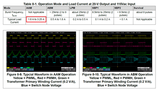
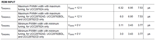
Regarding the measurement conditions in Figure 8-9 on page 16 of this document, the Load Current is described as "1.8A to 3.25A".
How many amps was the waveform in this figure actually measured at?
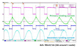
Also, are the conditions for other waveforms, including this waveform, as shown below? (Figure 8-9 to Figure 8-14)
Input:115VAC
Output:20V

The background of the question is below.
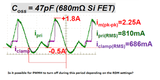
I am developing a power supply with an output power of 60W, but currently the efficiency is not very good.
It seems that the MOSFET for the active clamp has a large loss (it actually generates a lot of heat), and I believe that more current is flowing to the Hi side than necessary.
I think the on time of the Hi side switch is probably longer than it should be.
I also assume that the switching frequency is lower than it should be, and unnecessary current is flowing through the primary side.
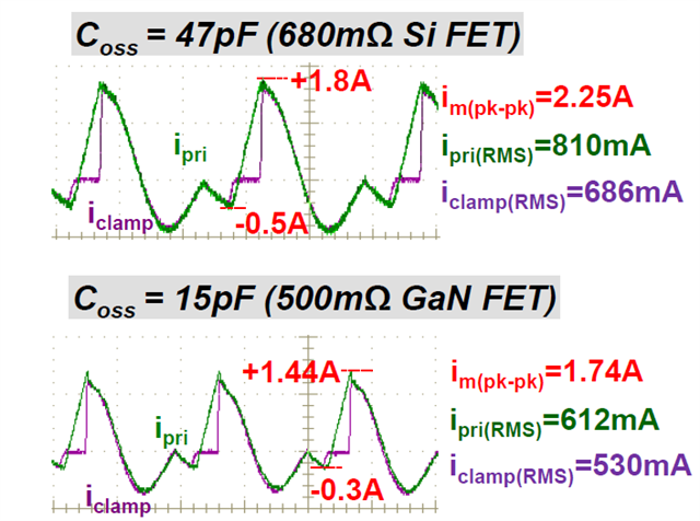
If the waveform in Figure 8-9 of the EVM data is a 60W output waveform, I think the primary side current can be compared between the circuit I'm considering and EVM.

Best regards,

  • Hi Kaji-San,

    Thank you for reaching out. 

    From the waveform shown for primary side current, I think the testing is done at 3.25A. Because running a small approximation can confirm this. The current probe is 0.2V/A and peak of primary current is around 450mv (green waveform), turns ratio is 5. So roughly, 0.5Ipk*Dmag*Nps = Iout, Dmag roughly is 0.57, Substituting these values gives 3.3A and this is taken at 115Vac and 20V output.

    Regards,

    Harish

  • Thank you for your reply.
    Attach the waveform.
    Is there anything you are concerned about regarding the behavior of this waveform?
    I predict that the Tz optimizer is not working properly, so the Hi-side on period is getting longer and the primary winding current is flowing excessively.
    I assume that this is the reason why it is not efficient.
    Best regards,

  • Hi Kaji-San,

    Yes, I agree with you, ON time of the high side switch has to be more to allow resonance to complete and negative Imag to cause ZVS. I think you will have to tune the RDM and RTZ resistor to improve this behaviour.

    Regards,

    Harish

  • Thank you for your reply.
    In addition, I would like to ask questions.
    What are the conditions for PWMH to turn off?
    Also, does the PWMH on time depend on the resistance value of the RDM pin?
    On page 80 of the datasheet, it is stated that reducing the resistance of the RDM pin will reduce the on-time.
    However, I cannot find a detailed description that specifies the on-time.
    Later, in the waveform I measured, the primary winding current flows at a maximum of about 2A during the PWMH on period.
    Could you please give us your opinion on the cause of this excessive current flow?
    Is it affected by the switch node capacitance energy being too large?
    Best regards,

  • Hi Kaji-San,

    Thank you for reaching out.

    Yes the PWMH ON time depends on the RDM resistor value selection. 

    (1) RDM pin sets initial TDM

    (2) Fine tune TDM to make QL turn around a given ZVS tuning target. This is done internally

    So approximately we can say the following:

    Tdm ~ (Vcst+ delV)/(NVo x Rcs/ Lm), So delV is internally adjusted to help ZVS.

    Excessive currents can be due to switch node capacitance as seen below:

    I think RDM and RTZ needs to be optimized.

    Regards,

    Harish

  • Thank you for your reply.

    Is the initial time of TDM calculated using the formula excluding ΔV?
    Also, is it okay to use the electrical characteristics in the data sheet below for the adjustment time of ΔV?

    The waveforms have Coss of 15pF and 47pF, but are these values the Coss of the low-side FET?
    Or is it a combination of the high side switch and low side switch Coss?
    Also, are the other parasitic components the same? Are the input and output conditions the same?

    Is it possible for PWMH to turn off at the following timing depending on the RDM settings?
    Presumably, if current is flowing to the secondary side at this timing, it will not turn off, but if no current is flowing to the secondary side, it will turn off.

    Best regards,

  • Hi Kaji-San,

    Yes, the initial estimate is calculated with the auto tuning consideration. 

    The electrical characteristics table can be used to correlate with the results seen and tune RDM to ensure it is within the max times of PWMH on time. Initial TDM setup is based on Equation (10) for RDM which is fine tuned along with RTZ usually at full load and high line to make sure ZVS can be achieved. After such a tuning, UCC28782 can make adaptive ZVS with auto-tuning for other operation conditions and modes.

    This is only of the low side FET and all other parameters and test conditions are maintained the same. 

    The PWMH signal, which drives the active-clamp transistor, is also indirectly modulated based in part on the demagnetization time (determined by the peak primary current, the output voltage, and the turns ratio) and in part by any additional time needed to generate negative magnetizing current based on the input voltage. So if, commutation of current is over to secondary, it could turn off after the propagation delay.  Then the resistor on the RTZ pin  programs the minimum tZ time, which is the sum of the propagation delay of the high-side driver and the minimum resonant transition time of VSW falling edge to turn on the low side switch.

    Thank you

    Regards,

    harish

  • Thank you for your reply.
    To understand TDM, please tell me about the following.
    Regarding the formula you taught me.
    What does N mean? Is it NPS?
    Vcst seems to be the current flowing through the low-side switch, but does it mean the peak current value when the low-side switch is on?

    Also, is the time stipulated by RRDM calculated using Equation 11 of the data sheet equal to the TDM above?
    Best regards.

  • Hi Kaji-San,

    Yes, N refers to the primary-Sec turns ratio.

    Yes, it will b the peak value of current when the low side switch is ON

    Yes, the resistor value formula is same as the one used in calculator and datasheet equation 11.

    Thank you

    Regards,

    Harish