This thread has been locked.

If you have a related question, please click the "Ask a related question" button in the top right corner. The newly created question will be automatically linked to this question.

TPS7B7702-Q1: Reverse Current Detection and Overcurrent Protection

Part Number: TPS7B7702-Q1
Other Parts Discussed in Thread: TPS7B7702,

Tool/software:

Hi,

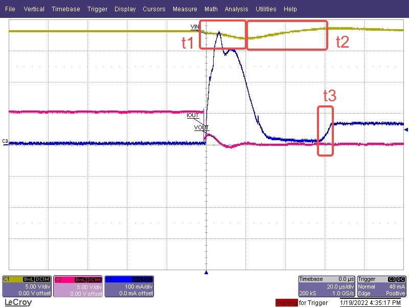
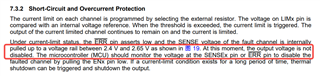
According to the datasheet, when TPS7B7702 is used for the dual-channel antenna LDO application, if one channel is shorted-to-ground, the temporary dip in the Vin can trigger the reverse-current detection fault and other channel will be latched off.

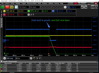
1. Now we have a 50uF inoput capacitor, and Vin=Vout1=Vout2=12V. When Vout1 is short to ground, Vin has a temporary dip of about 0.6V, triggering reverse-current fault in channel 2 and causing it to shut down.


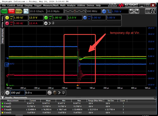
    According to the datasheet's provided output current and corresponding dropout voltage, the on resistance is approximately 500mV/100mA=5Ω, and the reverse current can be calculated as -0.6V/5Ω=-120mA ( <-40mA, Irev_typ). Does this mean that to avoid this false trigger event, Vin_dip needs to be less than 40mA*5Ω=200mV? How large of an input capacitor is needed to prevent this fault?


Ps: It was found that even a 400uF capacitor could not prevent this from happening. According to the calculation of ic=C*du/dt, the required capacitor would be extremely large and cannot be applied in the design.

2. When the output is held short-circuited, TPS7B7702 will continues to remain corresponding channel on, and the output current is limited. Dose this mean the internal MOS remains on? and the input voltage will remain low impedance to ground through the on-MOS ? If so, why doesn't Vin keep decreasing? What happens in that "temporary dip"?

Thank you!

  • Hello, 

    The on resistance will vary by temperature. 5Ω is associated with the worst case scenario. It can actually be less though as shown in Figure 7 of the datasheet. Assuming you'll be at or above 25C, you can expect on resistance to range from ~3Ω - 5Ω. Depending on the temperature of the junction, the dip would need to be below 120mV - 200mV (typical). 

    Is yellow the VIN to the LDO? How much dip is currently being observed?

    When a device like TPS7B7702-Q1 experiences short-circuit, it quickly starts to regulate current rather than voltage. Depending on where current limit is set, the MOSFET will be regulated to provide the current limit value. For example, if VIN = 12V and current limit is set to 200mA, then the MOSFET will become 60Ω during a short circuit event. However, this takes some time since the LDO needs to react to the load transient event.

    ~ Aaron

  • Hi Aaron,

    Thanks for your reply.

    1. Yes, the yellow is the Vin and the dip is about 0.6V.

    Do you have any suggestions to avoid this fault without changing the input and output voltages?

    2. Now I understand. I didn't take the 'current limit' into account before.

    Regards~

  • Hi Aaron:

    How long time it takes for the chip to react to a short circuit event? 

    And is it related to input capacitance?or is it a specific time fixed inside the chip?

  • Hello Lelian,

    Typically it takes 10's of us for the current limit loop to react. You can see this thread for a measurement that my colleague made: https://e2e.ti.com/support/power-management-group/power-management/f/power-management-forum/1099810/tps7b7701-q1-response-time-for-short-circuit-and-overcurrent-protection

    It's not related to input capacitance. It's more dependent on the internal current limit loop of the device and cannot be sped up. 

    ~ Aaron 

  • Hello Xiaochen,

    This is difficult since VIN and VOUT are close together. If VIN cannot be raised, then the only option is to try to increase the amount of capacitance on VIN to supply the temporary current being demanded by the short. 

    ~ Aaron

  • hi Aaron:

    I quoted the scope shot from the link you attached.

    Let's say t1 is the declining period time of input voltage, and t2 is the recovering phase. What's happening during t1 is RC discharging, since output is short to GND, the input capacitor and mosfet turn on resistance inside chip make up a RC discharging circuit. The input voltage stops dipping because the over current protection is triggered by the chip. And during t2, LDO starts to limit output current to low value, and the input voltage is recovering because of dynamic response of pre power supply circuit. At the end, t3 is the time LDO needs to regulate short circuit current.

    Am I understanding correctly?

  • Hello Lelian,

    You are pretty close in your interpretation.

    During T1, the input capacitor is indeed discharging since the upstream voltage source may have some impedance and is unable to provide all the current being demanded at the output. You're correct that T2 is where the current limit loop is reacting and changing the RDSON of the FET to be much higher. It's not until T3 where current is being regulated to its set value. 

    As you can see, the current limit loop needs some time to react and then settle to the set value. 

    ~ Aaron