This thread has been locked.

If you have a related question, please click the "Ask a related question" button in the top right corner. The newly created question will be automatically linked to this question.

UCC5870-Q1: DWJQ1

Part Number: UCC5870-Q1

Tool/software:

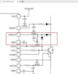
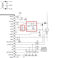
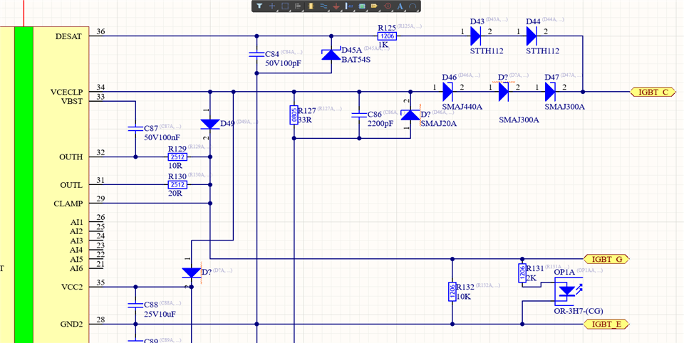
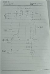
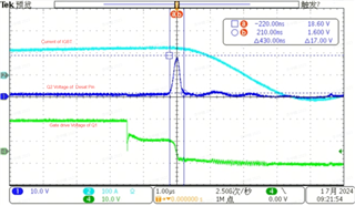
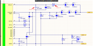
Hello, we recently used a gate drive chip UCC5870-Q1 when the active clamping function is triggered, the chip will heat up and even damage (active clamping pin VCECLP resistance becomes about 10 Ohm).
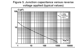
Your company's reference design does not protect the pin, I would like to ask you how to deal with the pin? Is it possible to add TVS between the VCECLP pin and VEE2, what is the recommended clamp voltage TVS?Thank you!

  • Hello Huajian,

    Could you share waveforms of the transient, and your schematic?

    The VCECLP pin is a high impedance input, and does not sink current, so the power dissipation is not through this pin. There still be extra power dissipation through the OUTL pin during a clamping event, but when used to clamp short transients this should not cause an issue since the power switch takes most of the energy. What are your register settings, and how are you testing this feature?

    Regards,

    Daniel Norwood

  • Hi,Daniel,the  schematic is the as demo board, except we changed 1.5 Ohm to 4.7 Ohm. We use IGBTs as overcurrent protection devices in series in high voltage circuits. We short-circuit the IGBT rear stage and then control thee IGBT to close so that overcurrent protection is triggered and active clamping is initiated. The high voltage at the moment of IGBT disconnection should cause damage to the VCLEP pin even though it's  impedance input?
    ?


  • Huajian, 

    Which demo board do you mean? Could you share the part number?

    There should be no current through the VCECLP pin, so it should not heat the device up unless there is a voltage on the pin beyond the datasheet abs max.

    Are he part numbers of the VCECLP diodes the originals from the demo board? Does the IGBT also get damaged? What is the voltage scale in the waveform?

    The damage you describe is not the expected VCECLP clamp behaviour, and I have not seen it before.

    Regards,

    Daniel Norwood

  • Daniel,

    The schematic is as follows.Now,we add a TVS SMAJ20A near the c86,and change the gate resistance from 4.7ohm to 10ohm and 20ohm and the gate driver chip no longer heat and damage.

    The IGBT  has not been damaged. The voltage scale in the waveform is 500V/div,the max voltage of the waveform is about 1500V,the max current of the waveform is about 320A.So the VCECLP should be subjected to a very high voltage.

    The VCECLP diodes are two SMAJ300A and one SMAJ 440A.

    So how should VCECLP pin be protected?

  • Hi Huajian, 

    The diode D49 in the circuit should shunt current from the VCECLP pin to turn on the gate, see section 7.3.5.7 of the datasheet. What are the specs on this diode? Based on what you describe, it seems like this diode is not working properly to turn on the gate. I assume you are testing with the IGBT connected?

    Could you share a waveform of the VCECLP pin during the overvoltage event?

    Regards,

    Daniel

  • HI Daniel,

    We are testing with the IGBT connected. The diode D49 is 1N4148. Is the response speed of this switching diode not enough to cause this problem?

    Should we replace it with a Schottky diode?  We did not capture the waveform of the VCECLP pin during the overvoltage event .

  • Hi Huajian,

    It is hard to give a strong recommendation without the VCECLP waveform. I don't think D49 is enough though, it is only rated for 2A surge, and the VCECLP circuit can easily exceed that. I would recommend trying a Shottky diode, and then when you test it capture the VCECLP waveform

    -Daniel

  • HI Danniel:

    The chip no longer heats up after the Schottky diode is replaced. But now we have encountered a new problem, that is, it is easy to mistakenly trigger desaturation when triggering overcurrent protection(320A threshold). The desaturation detection filter parameters are 1k and 100pf, and the diode is two STTH112. The IGBT model is SKM400GM17E4. Do you have any suggestions?

  • Hey Huajian,

    Daniel is currently out of office and will return later this week. Please expect a response from him by the end of the week.

    Thank you for your patience.

    William Moore

  • Hi Huajian,

    I am glad that solution was effective, and my apologies for the delay!

    For Desat, could you share the register settings you are using? What is the charging current, desat threshold, and deglitch setting?

    Typically adjusting these allows a balance of fast detection and no false reports. 

    Beyond that, if you can share a waveform with the desat pin, the gate, the nFLT1 pin, and the drain-source of the IGBT i can further help diagnose.

    Regards,

    Daniel

  • Hi Daniel,

     The charging current is set to 1mA,  desat threshold is set to 9.5V, and deglitch setting is set to 158ns.

     Because the equipment is installed in the whole machine, it is not convenient to test the waveform

  • In addition, can the desaturation function be disabled from the software?

  • Hi Huajian,

    If the waveforms cannot be tested how do we know this is not a real short circuit event that the desat circuit is detecting?

    Desat can be disabled in software by setting CFG4[DESAT_EN] = 0b.

    Regards,

    Daniel

  • Hi Daniel,

    Because we also have a level 1 hardware overcurrent protection, the current threshold is 320A. When the short circuit fault occurs, we now use the oscilloscope to measure the maximum current value in the loop is about 350A. So desaturation should not be triggered. We want to set the desaturation current value to about 1000A. Is our parameter appropriate now?

  • Hi Huajian,

    It is really hard to give recommendations without good waveforms. At first look the values you share look good. It is possible there is something in the layout leading to coupled transients, or it is possible there is a drain-source spike causing desat to report.

    For the 350A current measurement, were you probing the inductor current, or power switch current? Often shoot through events do not show up at all on the inductor.

    Regards,

    Daniel

  • Hi Daniel:

    We now test such a working condition, a current of more than 100 A is passed into the loop, and then the software controls Q1 to turn off, at this time Q2 also triggers desaturation, and the waveform is shown in the figure. (Green is the grid voltage of Q1,Blue is Q2's desat pin voltage). Filter resistances and capacitors are 1k and 100pF.  What do you suggest?

  • Hello Huajian,

    I see two posabilities:

    1. The source emitter voltage of the IGBT is actually going above the configured threshold while the output of the gate driver is on (GATE is high). IN this case the desat circuit as working as expected, and we need to figure out why there is a source emitter spike, or increase the filter on the desat pin.

    2. The desat diode capacitance is leading to injected current when Q1 turns off. This would be due to DV/DT across the Q2 IGBT injecting current through the diode capacitance (I=C*dv/dt). This can cause spike like you are seeing. To test this i recommend a diode with a lower parasitic capacitance, or putting two diodes in series to reduce the parasitic capacitance. This will reduce the spike. 

    Regards,

    Daniel

  • Hi Daniel,

    Now ,the charging current is set to 0.6mA,  desat  threshold is set to 9.5V, and deglitch setting is set to 316ns.and the filter resistances and capacitors are 2k and 330pF.After this modification, the phenomenon of false triggering desaturation will no longer occur. Two diodes  STTH112 were originally used, and its junction capacitance parameters are shown in Figure.  Will this parameter setting cause a large desaturation delay?

  • Hello Huajian,

    These parameters will slow down desat detection, but typically that is okay with IGBTs, as they are not as sensitive to desat events as SiC devices. 

    -Daniel