This thread has been locked.

If you have a related question, please click the "Ask a related question" button in the top right corner. The newly created question will be automatically linked to this question.

TPS54561-Q1: Transient Current Load Response

Part Number: TPS54561-Q1

Tool/software:

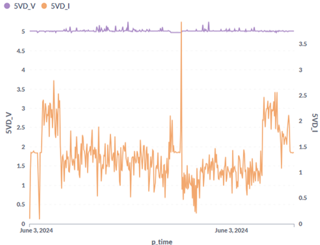
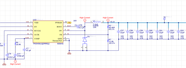
Hi, a quick one on the TPS54561-Q1. My load is a bit noisy and the current can bounce around by a delta of up to 2A in 200-500ms. The regulator handles this pretty well, but I still see a ripple response on the rail of up to +/-400mV and am wondering what is the best part of the design to tune to minimise this essentially transient step response ripple? Many Thanks.

  • Hi Dave,

    This could be due to the way the measurement is carried out. In order to obtain actual output voltage ripple, it is imperative to minimize the measurement loop during the measurement set-up.  I recommend you to go through TI APP note " How to measure ripple for better design outcomes"

    Even after proper measurement, if you still see issue i recommend you to share Vout ripple, Inductor current/ Iload waveforms and TPS54561-Q1 device schematic. 

    Thanks,

    Nitya

  • Thanks Nitya, these measurements are coming from an ADC very close to the converter output so we wouldn't expect to see any noise due to measurement error as in the app note you mentioned. When this noisy current load is not present the rail is perfectly clean and rock solid.

    This is a plot of the 5V voltage rail (purple) and current profile (orange). You can see the current is bouncing around a lot, and as a result the 5V has transient spikes up to 5.4V. It is these spikes that we are trying to minimise. They are always high side for some reason, we don't seem to see similar spikes below 5V.

    This is our schematic, as you can see we already have a large amount of capacitance on the output. Have you got any advice for tuning this transient response to the noisy current load to minimise the essentially overshoot on the 5V rail? Is adding more output capacitance or increasing the switching inductance our best option? Or is there something we can do with the control loop frequency compensation? Thanks.

  • Hi Dave,

    Thanks for the plots and the schematic. I just updated the design excel file if i can optimize the compensation values for better time response. As per the design, the comp values are already optimized for better time response. If you still optimize the Comp values for higher Fcr the phase margin will reduce and it is not recommended.
    I have attached the excel file that i have used, please go through it and let me know if you have any doubts.

    /cfs-file/__key/communityserver-discussions-components-files/196/TPS54561-design-calculation.xls

    I still feel issue is due to ADC measurement. The best way is to probe the output voltage across the output capacitor. However if you are very confident about ADC measurement accuracy, then only way is to increase the output capacitor values to higher values and adjust compensation values accordingly to resolve this issue.

    Thanks,
    Nitya

  • That's great Nitya, many thanks for the Excel file. I'll do some more work to confirm the ADC isn't exacerbating things.