This thread has been locked.

If you have a related question, please click the "Ask a related question" button in the top right corner. The newly created question will be automatically linked to this question.

UCC23511-Q1: Using Isolated Gate Driver to Drive FET's in High Side back to back configuration

Part Number: UCC23511-Q1
Other Parts Discussed in Thread: BQ79616, UCC23511

Tool/software:

Hey TI Experts,

We are designing a system for Bi-directional current flow to and from a Battery Pack.

Hence, we have the FETs on the high side arranged in back to back topology with Sources of the Discharge and Charge FETs common.

The following are the points in which we require clarity:

1)In order to drive the gate of the FETs in high side we've used an Opto-coupled Isolated gate driver through which the source terminals are isolated from the logic side.

We've used an isolated power supply specifically for this purpose.

2) We have used a pre-discharge circuit consisting of a P channel FET in series with current limiting resistors. Hence, as the Pre-discharge FET is connected in parallel with the discharge FET and as the P channel FET requires lower potential at gate terminal than source terminal. Thus, we've used another opto-coupled isolated gate driver for achieving the same by referencing gate to ground and source to the PDSG control pin.

We would like to know if the circuit will work optimally or are there any optimizations or changes needed.

Awaiting your valuable response on the same.

Thanks & Regards

Ibrahim

32'S_BMS-Gate_Driver_Current_Sense (2).pdf

  • Hi Mohammed,

    This question is a continuation of this thread: https://e2e.ti.com/support/power-management-group/power-management/f/power-management-forum/1371796/ucc37324-driving-fets-in-high-side-configuration-with-low-side-gate-driver In the future, just reply to the original post with follow up questions. This helps streamline our debug efforts.

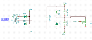
    Which is that PMOS? Is it the one in the PDSG circuit box? Don't connect OUT to the PMOS drain. You can drive the PMOS gate with OUT normally, and use a negative voltage on the gate driver's VEE for turn ON. You just need to reference VEE to the PMOS "bottom/drain using a simple Zener circuit, such as the one below.

    Best regards,

    Sean

  • Hey Sean,

    Thanks for the swift response. 

    I would like to give a more detailed description of the circuit we've designed which are as follows:-

    1. The application of the circuit is for a BMS using the BQ79616 AFE. As the AFE doesn't have the control pins for FET switching, we are doing it through the MCU.

    2. The DSG pin depicts the discharge pin and CHG is the charge pin, PDSG is the Pre-discharge pin.

    3. As per standard operation when the load is connected for the 1st time the PDSG i.e., the P-channel FET is active to limit the inrush current. The PDSG pin remains on for few seconds after which the switching transitions to the DSG pin and then the PDSG pin is switched OFF.

    The points we need more clarity on are:-

    1) To drive the P channel FET we need negative potential at the gate with respect to source. As per your explanation the UCC23511 has an output voltage i.e., Vcc - Vee of 10 to 33V. So how is it possible to execute the concept you explained with this part. 

    Or we might have failed to understand the circuit you explained.

    Or is there a part which fits the criteria. We would like to know more on the same.

    Awaiting your kind response on the same.

    Thanks & Regards

    Ibrahim

  • Hi Ibrahim,

    I'm sorry, I made a mistake in my schematic; I am not used to PMOS. I have corrected below. You are right, you need a negative potential at the gate with respect to the source. My main point is that you can generate a negative voltage at VS- by referencing the isolated supply to the PMOS source. You still want to use OUT to drive the gate.

    Best regards,

    Sean

  • Hey Sean, 

    Thanks for the clarification.

    One more tapping from the Source needs to be taken and connected to Bat+ right?

    Also is the isolated gate driver suitable for this kind of operation?

    Thanks and Regards

    Ibrahim 

  • Yes, you could short out R7 alternatively. Otherwise you will just have a postive turn-off supply. This might help the switch turn off faster, and maybe prevent false turn-on if a strong negative transient is injected into the gate, due to high negative dVds/dt when the switch is open (Miller injection).

    Best regards,

    Sean

  • Hey Sean,

    Understood. Appreciate your response.

    Is our present circuit also ought to work fine or is there a flaw.

    Also, can N channel FET be used for Pre-discharge in parallel with the main DSG FET? 

    Because I haven't come across any material or resource where N channel FET is used for Pre-discharge. If true then what might be the reasons?

     I've attached the Schematic with N channel FET used for Pre-discharge.

    Please let me know if this will work and downsides if any with this concept.

    Thanks

    Best Regards

    Ibrahim 

    .32'S_BMS-Gate_Driver.pdf

  • Hey Sean,

    Understood. Appreciate your response.

    Is our present circuit also ought to work fine or is there a flaw.

    Also, can N channel FET be used for Pre-discharge in parallel with the main DSG FET? 

    Because I haven't come across any material or resource where N channel FET is used for Pre-discharge. If true then what might be the reasons?

     I've attached the Schematic with N channel FET used for Pre-discharge.

    Please let me know if this will work and downsides if any with this concept.

    Thanks

    Best Regards

    Ibrahim 

    .7144.32'S_BMS-Gate_Driver.pdf

  • Hi Mohammed,

    An NMOS has lower resistance than a PMOS. If you have an isolated supply, you might as well use an NMOS. A PMOS is easier to turn on at DC when you do not have an isolated supply. 

    The schematic looks good to me. Just make sure you setup the supply rails with the correct voltages and sufficient current.

    Best regards,

    Sean