This thread has been locked.

If you have a related question, please click the "Ask a related question" button in the top right corner. The newly created question will be automatically linked to this question.

BQ25895M: Question about detecting input source

Part Number: BQ25895M

Tool/software:

Dear TI experts,

My customer tests BQ25895M in their own PCB, and there is a problem of detecting input source.

They are testing with HP laptop, and some ports have a problem detecting CDP. The scenario is as below;

1. Connecting VBUS to specific USB port of laptop

2. detects CDP (DSEL pin is 0), charging starts

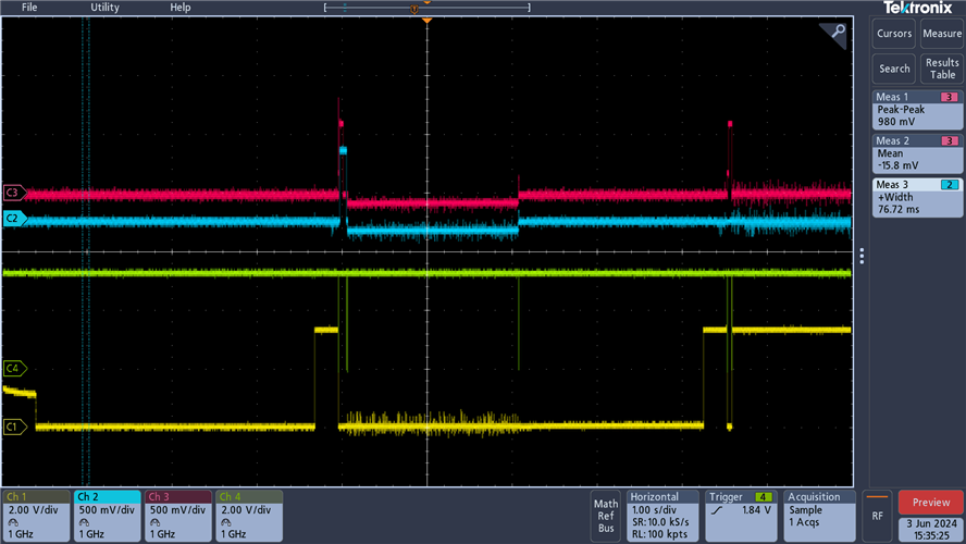
3. STAT pin becomes to 1 (charging stop), and check the input source again, and detects SDP (DSEL pin is 1).

4. If the charging stops, VBUS also becomes to 0V and after change to 5V.

5. As I described above, DSEL pin is 0 when CDP is detected, DSEL pin is 1 when after SDP is detected.

I attach the waveform for your convenience. RED is D+, BLUE is D-, GREEN is INT, YELLOW is DSEL.

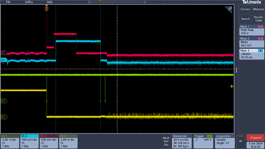
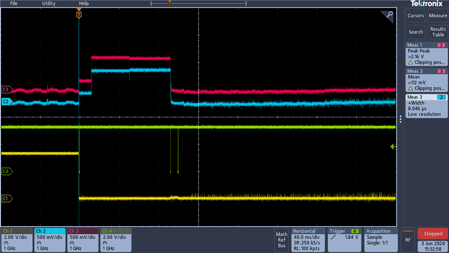
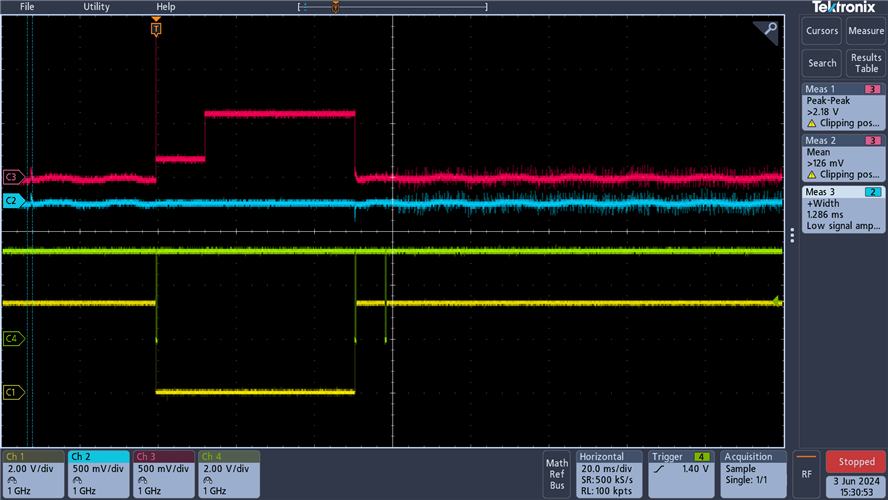
I also attach the waveform of nomal operation

- Detectiong CDP normally

- Detecting DCP

- Detecting SDP

And customer's register setting is as below.

Reg 0x06 : 0x5E

Reg 0x00 : 0x1C

Reg 0x02 : 0x31

Reg 0x03 : 0x1A

Reg 0x05 : 0x13

Reg 0x07 : 0x8D

Reg 0x0D : 0x95

Here is the schematic. Please check it just in case.

Print.pdf

Please check this issue, and let me know if you need more information about it. Thanks.

Best regards,

Chase

  • Hi Chase, 

    Please see my comments below. 

    On BQ25895M it is known behavior that DSEL pin remains low when either CDP or DCP is detected. For all other detection results DSEL will return high when D+/D- detection is complete. The waveforms provided match the expected DSEL behavior. 

    The BQ25895M has a limitation regarding detecting CDP. Some USB ports, typically on a notebook or PC laptop, require a pull up on D- within approx. 2 seconds to confirm CDP detection. The BQ25895M does not force this pull up and when the pull up does not occur the USB port (on the source side) will briefly shutdown and then reconfigure as SDP. 

    It appears this is what is occurring in the customer's system with certain laptop ports. Unfortunately this detection behavior cannot be modified from the perspective of the charger IC. The customer can override the 500mA input current limit set for SDP via I2C write to REG00.  

    Best Regards,

    Garrett 

  • Dear Garrett,

    Thank you for your support.

    I have more questions about your answer.

    1. You said that some USB ports on a notebook or laptop require a pull up on D+. Can I know which USB port require a pull up in advance? As you know This is not random behavior, only certain port have this behavior. and on another laptop, only other certain port have this behavior. My customer tested 5 laptops which are same brand, same model. Each laptops have same symptom, but the location of USB port that have this symptom is different.

    2. Regarding the pull up on D+, Is it the perfect solution for detecting CDP? Do you have a value of pull up resistor?

    How about D-? Does not D- need pull up?

    3. You said that BQ25895M has a limitation regarding detecting CDP. It sounds like other chargers do not have a limitation detecting CDP. Could you recommend other charger IC which does not have limitation detecting CDP and have a 3A boost converter inside?

    Best regards,

    Chase

  • Hi Chase, 

    Please see my comments below. 

    1)Unfortunately I have no additional information to help distinguish what specific USB ports require a pull up. The documentation we have states some CDP ports do not require the additional pullup on D-, while others do. The BQ25895M is able to detect CDP ports which do not require the additional D- pullup. You will need to get relevant information on USB ports from the laptop manufacturer.  

    2)Apologies I misspoke in my initial response (now corrected) the voltage pullup expected to confirm CDP is 0.5V to 0.7V on D- line and at that time D+ should remain below 0.4V. 

    3)Unfortunately I do not have a more appropriate alternate part to recommend. We have a few newer single cell buck parts than the BQ25895M, but they do not support 3A boost converter and D+/D- detection. 

    Please allow me to also propose an alternate workaround option. The customer could modify their MCU firmware such that when a new input adapter is initially detected as CDP and then power cycles and re-detects as SDP they can override the IINLIM setting in REG00 from 500mA to 1.5A to achieve the higher charge current of a CDP input. 

    Best Regards,

    Garrett 

  • Dear Garrett,

    Thank you for your support, and hope you had a good weekend.

    1. My customer had a test that applying 3V on D+ after CDP adapter is detected, and they found that it is working well.

    (but your saying is that it is pull up on D-, not D+. Am I right? I will ask my customer to test again.)

    2. Again, Do you have any reference circuit for applying 0.5V to 0.7V on D- if CDP is detected? And if I apply this reference, Is there any problem to detect other types of adapter like DCP and SDP?

    3. Unfortunately I could not find the information about needing pull up on D- line or applying 0.5V to 0,7V on D- line if CDP is detected in the datasheet. Could you guide me about this document? or it is not updated yet in the datasheet of other documents?

    4. In the description of DEL(pin24), it looks like DSEL pin goes to high (after detection is complete) by external pullup resistor except MaxCharge adapter is detected. (on the other hand, DSEL goes to low if MaxCharge adapter detection is done)

    As I posted initial question, DSEL pin is goes to low if CDP is detected in certain USB ports. You said that it is know behavior, Can I find it in the datasheet or other documents? or Is it not updated yet in the document same as question no.3?

    Please check these issues. Thanks.

    Best regards,

    Chase

  • Hi Chase, 

    Please see my comments below. 

    1) I am referencing the BC1.2 standard. The documentation I have available to me outlined CDP detection confirmation expected 0.5V to 0.7V on D- line and at that time D+ should remain below 0.4V for secondary detection. I am not able to guarantee exactly what will work on the various laptop ports the customer is testing. 

    2)Unfortunately I do not have a reference circuit to provide. Applying said voltage at proper time for secondary detection should not cause issues with detecting DCP and SDP. 

    3) TI does not provide specifics for each different type of detection in the datasheet. This is consistence across multiple charger IC families which have D+/D-. Please refer to documentation on BC1.2 standard. 

    4)DSEL pin expected behavior after D+/D- detection is complete is not described in great detail in the datasheet. 'Maxcharge' mentioned in current description is an extension of DCP, but expected DSEL behavior with CDP detection is not clear. Based on your feedback we will work to add this in the next datasheet revision. 

    Best Regards,

    Garrett