This thread has been locked.

If you have a related question, please click the "Ask a related question" button in the top right corner. The newly created question will be automatically linked to this question.

UCC27282-Q1: Power dissipation estimate and simulation results do not agree

Part Number: UCC27282-Q1

Tool/software:

I have been using slva504a to try and estimate the power dissipation of the FETs in an H-bridge being driven by the UCC27282-Q1 driver chip. I have a spreadsheet, when I use a very small load current like 12 mA. I get a very small power dissipation of around a 1 mW. 
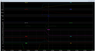
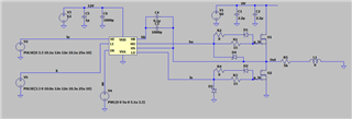
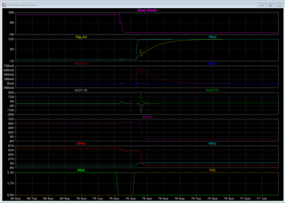
I wanted to verify my calculations using a spice simulation. I am using the UCC27282-Q1 driver to drive the top FET U1 and a bottom FET U2 into a resistive load of 5kohm. When I run the simulation, it looks like almost 20 Amps flows through U1 and U2 while Vout is transitioning from the High voltage bus voltage to ground and a similar but smaller spike occurs in the opposite direction. The current is not shoot through because I can clearly see the top FET turn off before the bottom FET turns on. The current seems to be flowing right before the miller effect plateau in the bottom gate voltage. Is this real / does this make sense or is it a simulation artifact ? I am not a FET expert. The result in the power estimate is that the bottom FET dissipates around 400 mW instead of 1 mW. I do not see anything of this order of magnitude in the application note because all the terms depend on the load current.  I have tried a couple different FETs. If this is real what phase does it map too in the application note? I would like to close the gap between simulation and my excel calculation. Purhaps I am using the wrong note?
Attached is the simulation results for the following edge of Vout. 
  • Hi / li are input PWM waveforms to driver
  • Ho / lo are output of the driver
  • Vout is the voltage at the 5k load. 
  • U1 is the top FET, U2 is the bottom FET. I have plotted the Source current of U1 and drain
  • I(R5) is the current to the resistive load. 
  • Ix(U2:G) is the current into the bottom FET.  g_lo is the voltage at the bottom FET gate, lo is the output of the driver (I have the standard resistor in parallel with resistor diode filtering on the gates. 

  • Hey Jennifer,

    Thank you for reaching out to TI regarding your question with the UCC27282-Q1.

    That application note comes from our motor drive team that utilizes a gate driver with integrated power FETs.

    When looking at your waveforms, it is best to measure HO with respect to HS using a differential probe to see more clearly the Vgs of the FET.

    Also, during this situation, could you measure HS as well?

    On the EN pin, what is the pulse generator doing there? EN needs to stay high during operation.

    Is this during steady state operating condition?

    Let me know if you have any questions.

    Thank you,

    William Moore

  • Thank you for the quick response. 

    I have added ho-hs to the plot. hs = out in this simulation.

    I start the simulation with the driver disabled and then turn it on, these are taken in steady state. 

    In looking at the current glitches on Ix(U1:S) and Ix(U2:D) it seems like maybe they are the Cds of the FET charging and discharging?

    The application note does not include this. 

    Can you confirm?

  • Hey Jennifer,

    Looking at this further, predicting power dissipation through simulation does not yield very accurate results due to not all parasitic elements and resistances are accounted for. The high currents that you are seeing look like the Coos (Charging/discharging) current in the power MOSFETs.

    For determining power dissipation, you are better off utilizing traditional analysis and equations.

    Thank you,

    William Moore

  • Yes but in the past the traditional analysis did not match well with what we saw in lab. I was hoping simulation might show what we were missing.