This thread has been locked.

If you have a related question, please click the "Ask a related question" button in the top right corner. The newly created question will be automatically linked to this question.

LM5123-Q1: Bypass moe

Part Number: LM5123-Q1

Tool/software:

Hello, 

Regard the Bypass mode. 

Does it work for all input voltages as defined in the datasheet for boost (3.8-42v) ?  And does it also support 200W power transfer ? 

For example, my application in its regular operation shall boost voltage from 9v-12v in the input to 16v/10A on the output. Considering I configured the LM5123-Q1 to work 

that way but at part of the time the V-input will go high to 19v>16v? In that case will the device still support 16v x 10A =160W on the output? What will be the efficiency in that

case?  

Thanks,

Ohad

  • Hello Ohad,

    Thanks for reaching out to us via e2e.

    The LM5123 is a pure boost controller, so it can only regulate upwards.
    It is not a Buck-boost which could reduce the input voltage.

    So, when the input voltage goes to 19V which is higher than the regulation target, the LM5123 will go into bypass mode (if configured correctly for that mode).
    Bypass means that the high side FET will be permanently turned ON.
    Without the bypass enabled, both FETs will be OFF, and the current will flow across the body diode of the high side FET (causing losses and generating heat).
    In bypass mode, when the high side FET is ON, the voltage drop across the FET and the losses inside the FET will be lower.

    But the output voltage will be either 18.3 to 18.8V.
    It cannot get reduced / regulated down to 16V.

    So, a converter which is based on the LM5123 cannot (still) support 16v x 10A =160W on the output while the input voltage is 19V.
    Instead, you will see around 18.8V on the output ad it depends on your load which current will be drawn at that higher voltage.

    You have to choose the FETs in a way that they can permanently support this current.
    This is not a question of the controller.

    Best regards
    Harry

  • Hi Harry, 

    Thanks for the answer. I didn't mean it to be a buck, I asked exactly about the case you described which is: 

    1. When Vin=9v-12.5v the Vout will be configured o 16v - Boost functionality 

    2. When Vin=19v then Vout=~19v and Iout=Iin - Bypass functionality. 

    I just wanted to make sure the below: 

    1. Does the LM5123-Q1 device support Bypass for power transfer of 160W (V=10v, I=8.5A, off course it is on me to choose the right N-FET and Inductor) ?

    2. What configuration is required in order to enable it that LM5123-Q1 will automatically switch from Boost mode to Bypass mode and vise versa depending on the Vin voltage?  

    Thanks, 

    Ohad

  • Hello Ohad,

    All the controller does in bypass mode is that it will permanently turn on the high side FET.
    Therefore, this has no influence on the max power that you can draw.
    The external components (inductor, high side FET, sense resistor, etc.) will need to be able to deal with this DC current, that's all.

    To enable bypass operation, please connect the SYNC/DITHER/VH/CP pin to VCC.
    This will enable the charge pump for the high side gate driver:
    Datasheet page 5:
    Charge pump enable pin. If the pin is greater than 2.0 V, the internal charge pump maintains the HB pin voltage above its HB UVLO threshold for bypass operation, which allows the high-side switch to turn on 100% during bypass operation.

    When selecting the FETs, please be aware that the voltage which is delivered by the charge pump will be lower that the VCC voltage during regular operation (FETs switching):
    Datasheet page 27:
    Care should be taken when the converter operates in bypass at any conditions. During the bypass operation, the minimum HO-SW voltage is 3.75 V

    Best regards
    Harry

  • Hi Harry, 

    Thanks for the clarifications still some things not clear enough: 

    1. Does the connection of SYNC/DITHER/VH/CP pin to VCC shall be through PU like in EVM or straight to VCC ? 

    2. 

    When selecting the FETs, please be aware that the voltage which is delivered by the charge pump will be lower that the VCC voltage during regular operation (FETs switching):
    Datasheet page 27:
    Care should be taken when the converter operates in bypass at any conditions. During the bypass operation, the minimum HO-SW voltage is 3.75 V

    I don't understand how that can be taken care? These voltages are internal controlled by the controller. 

    When selecting the FETs, please be aware that the voltage which is delivered by the charge pump will be lower that the VCC voltage during regular operation (FETs switching):

    I don't understand that also. 

    Ohad

  • Hello Ohad,

    1.
    Please connect the SYNC/DITHER/VH/CP pin straight to VCC.

    2.
    The high side FET needs a gate voltage which is higher than the voltage on the source pins of the FET (switch node voltage).
    When the controller is boosting and the FETs are switching, the supply for the high side gate driver is taken from the capacitor on the HB pin.
    In that case, the supply voltage for the high side gate driver is voltage is around 5V (VCC voltage).

    But when the FETs are not switching, the capacitor on the HB pin will not get charged
    To support bypass mode (where the high side FET is always on), an alternative supply for the high side gate driver is necessary.
    For that purpose there is a built-in charge pump inside our controller.
    This charge pump will only generate a voltage as low as 3.75V above the switch node voltage.

    Therefore, please select FETs which will be fully turned on at a gate voltage of 3.75V.
    Otherwise the bypass mode cannot work.

    Best regards
    Harry

  • OK, You now emphasized here a very important point! 

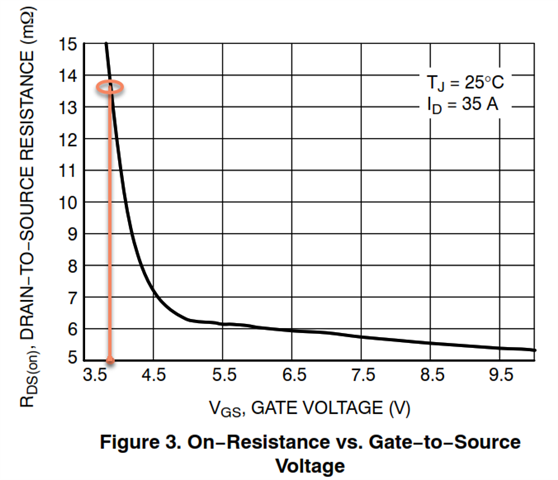
    I don't know if you are aware for the fact that the FET recommended by EVM which is the one I took has a very big Rds-ON at Vgs=3.75v :

    That means a very high dissipation in bypass mode which is : P=I^2*R= 8^2*0.014=0.874W. 

    In order to make the Bypass mode efficient, it needs a FET which on the one hand has a low switching loss and on the other hand a not high Rds-ON at Vgs=3.75v. 

    Why is it only 3.75v above the switch node ? 

    Ohad

  • Hello Ohad,

    First let me clarify one misconception.
    The EVM is meant to show different options and modes, allow to measure and to feed external signals and so forth.
    Therefore, it has all these jumpers and connectors.
    But it is not optimized in any way.

    It is far from being a golden sample or reference design to copy from.
    Also, please do not copy the layout of the EVM. Please follow the guidelines and the image in chapter 11 of the datasheet.

    On the EVM, we are using some standard FETs which are used on many other EVMs.
    So, these FETs are not optimized for all use cases or applications.
    These FETs are not "recommended" as the best choice for the LM5123 under all circumstances.

    There are technical reasons why the charge pump voltage is lower than VCC.
    The charge pump is fully integrated inside the controller IC, including all necessary capacitors.
    There is just not enough space to integrate a more complex charge pump with multiple stages.

    Anyway, this component does provide a real bypass mode which is still better than just a low IQ mode without bypass where the whole load current would flow across the body diode of the high side FET.

    Therefore, long story short, if your system will operate in bypass mode most of the time, please make sure that you will select an appropriate FET which only requires a low gate voltage.

    Best regards
    Harry

  • Hi Harry,

    Thanks a lot for that explain and clarification regard the EVM. Somehow it is thought that EVM is kinf of a "Golden" PCB. I agree I don't think that always but a lot of engineers like my colleagues believe it so it is very important to have that official clarification that it is not a "Golden". 

    BTY, so in a regular boost operation, the Vgs of the High MOSFET which is actually HO-SW is usually 5v since HO buffer is powered by VCC=5v which in turn powered by HB relative to SW?

    Thanks, 

    Ohad

  • Hi Harry, 

    Just wanted to be clear regard the Bypass mode: 

    1. How does the LM5123-Q1 gets into Bypass mode? Is it done automatically when Vin (The supply voltage) > Vload (The fixed output voltage configured by TRK resistors divider) ? That term is enough to put the device into Bypass mode? 

    2. What happens when Vin(supply voltage) = V-load(configured output voltage)? What mode will be that case? What output voltage? 

    Thanks, 

    Ohad

  • Hello Ohad,

    The high side gate driver is not directly powered by VCC.
    The supply for the high side gate driver is taken from the external bootstrap capacitor between the HB pin and the SW pin.
    While SW is pulled to GND (via the low side FET), this capacitor gets charged to VCC minus a diode drop.
    But there are usually some undershoots on the switch node, so that the voltage is a bit higher than that, basically about the same as VCC.

    When Vin is the same as the commanded output voltage, the controller will keep the output voltage at that level by skipping pulses.
    When one pulse delivers too much energy to the output, so that the output will rise too much, it will skip one or more pulses to allow it to decrease to the commended voltage again.

    When Vin is higher than the commended Vout, and the overvoltage status remain for at least 40 μs, the controller will automatically go into bypass mode.
    It will also automatically return to BOOST mode, when the input voltage falls again.

    See Chapter 8.3.18 in the datasheet for both these cases.

    Best regards
    Harry