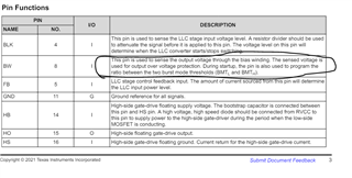
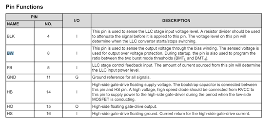
Other Parts Discussed in Thread: UCC25660
Tool/software:
Please answer the following questions regarding the UCC256403 device:
<Question 1>
UCC25640x LLC Resonant Controller
SLUSD90E – JUNE 2019 – REVISED FEBRUARY 2021
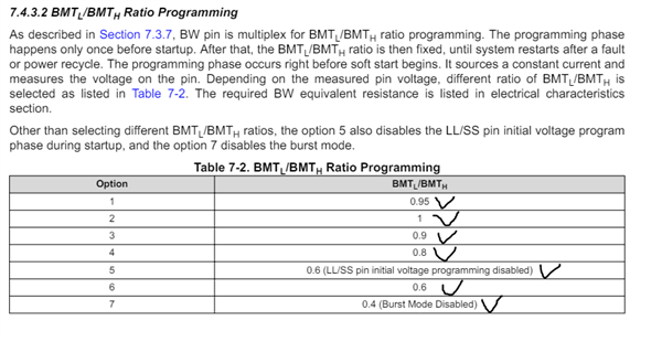
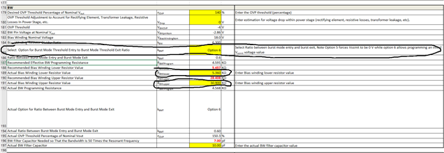
In the explanation of "7.4.3 Burst Mode Control" on page 36, the bottom of the page says,
"The Pick Higher block continues to function by selecting higher values of BMTL and FBreplica relative to the control effort Vcomp. In this case, BMTL limits the maximum switching frequency of LLC."
①What is the specific frequency that is limited?
②Also, it says that the condition for continuing control is to "select higher values of BMTL and FBreplica." Is this selection a setting that can be controlled externally?
If so, please tell me the specific setting method.
<Question 2>
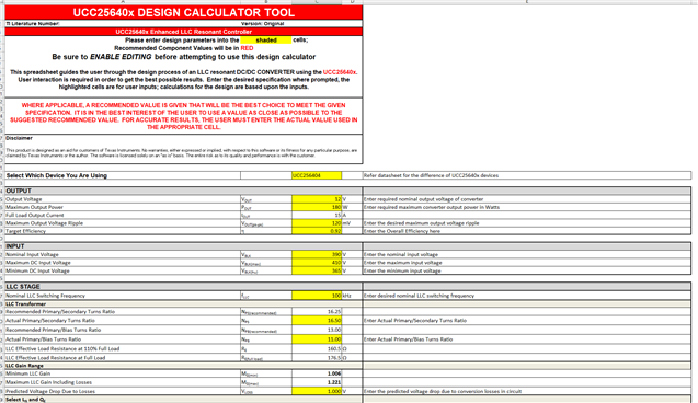
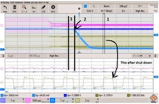
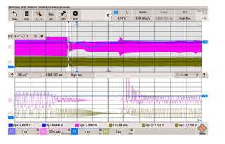
Due to the circuit configuration, I need control that does not use burst mode.
The current problem is that when the output voltage (-5% to -10%) is changed with almost no output load, the feedback control cannot respond at the control limit, and the FB terminal of this IC is sunk to GND by photocoupler control from the output, and the output voltage rises sharply from 4.9V to about 5.3V, becoming an unstable voltage.
A simple solution would be to connect the necessary dummy load, but this defeats the purpose of increasing conversion efficiency.
So, is there a way to stabilize and maintain the output voltage within a certain accuracy, like forward PWM continuous control, without using the IC's burst mode control, even at the limit of continuous control with a light load?
If possible, please let me know the specific solution.