Other Parts Discussed in Thread: LM5181, LM5180EVM-S05
Tool/software:
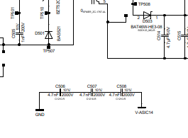
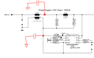
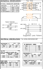
Transformer parameters
Hello Team,
I am using LM5181 for fuel cell monitoring application
Output voltage - 20V/40mA
Input voltage - 24V (6V-32V)
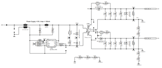
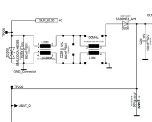
14 Number of similar fly-back circuit is used in 1 PCB. The input for all the fly-back are taken from the input filler(Figure-2).
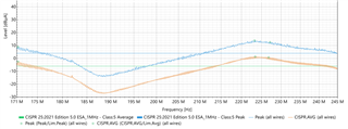
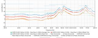
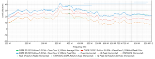
The conducted emission in voltage method looks fine (150K-108MHz) as per CISPER-25 (Class-5) limits. But radiated emission and conducted emission by current probe method is getting failed. The plots from measurements are below.
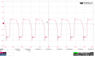
CP Test
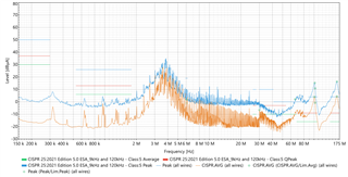
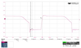
RE test
Can you suggest some steps to identify the route cause?
Is TI done EMI test on evaluation board as per CISPER25?

 .
.