This thread has been locked.

If you have a related question, please click the "Ask a related question" button in the top right corner. The newly created question will be automatically linked to this question.

TPS55010 failure

Other Parts Discussed in Thread: TPS55010

Hi all,

we are testing some samples of TPS55010 and we experienced some problems due to the systematic failure of low side NMOS (?). At the moment we built 7 prototypes and all failed in the same way.

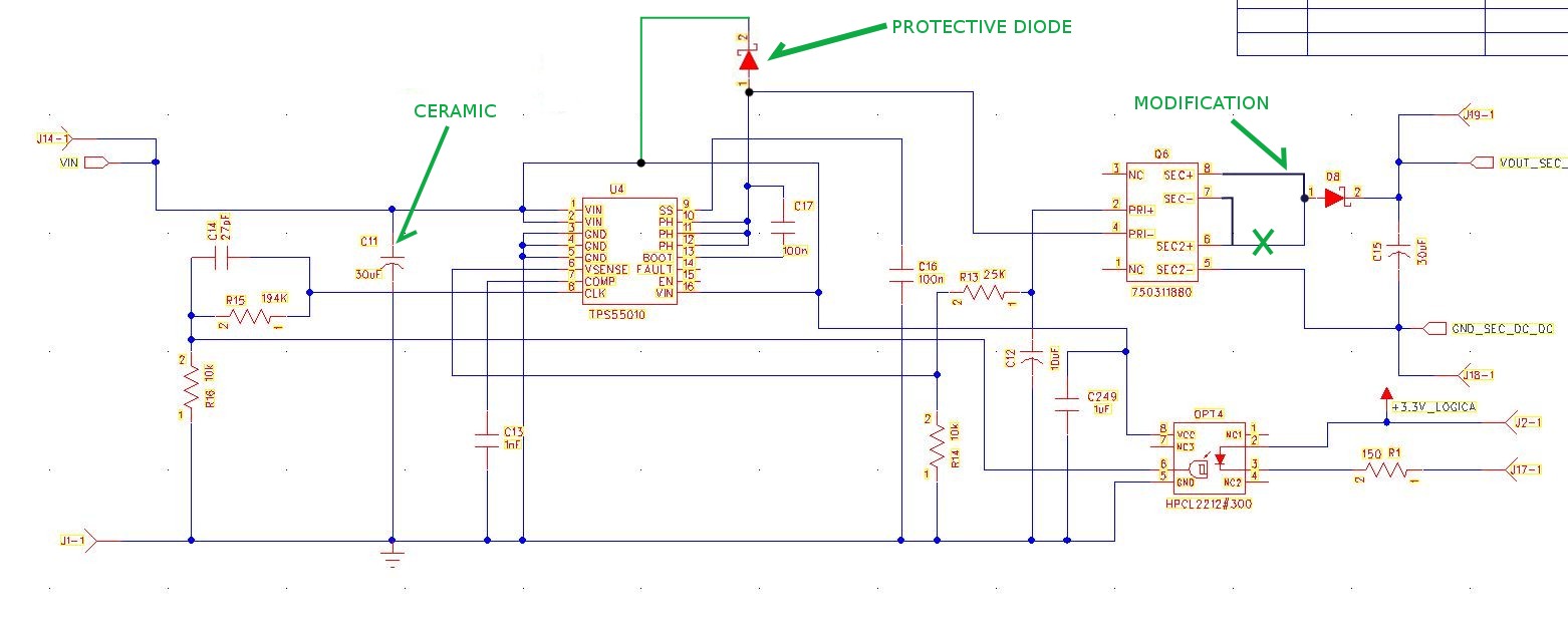
Is there some reason for such instability? We are using the schematic indicated in the datasheet with the magnetic from WURTH 750311880 (also suggested). The PCB looks like the ones indicated in the evaluation board.  
The device starts regularly but after a while (e.g. connecting the ground of the DSO to the board) it fails.
Are there some critical issues in the board layout that were not reported in the datasheet?
Any experience?

Gianpietro
Micromed-Italy


  • I apologize but I am having difficulty reading your schematic. Please attach a PDF of the circuit. FYI, I have attached the EVM schematic. There are differences which may lead to your issue.

    • Transformer hook up is different.
    • Input capacitance (need ceramic)
    • What is the opto for? EVM doesn't use an opto (I can't really tell which pins this is hooked to due the schematic resolution).
    PWR009A_sch.pdf
  • Sorry for the low quality. We will provide the pdf. The transformer is connected in fly-back mode in both circuits, our and EVB (in one the ground is up, in the other ground is down but our picture is too lowres to see this, sorry). The transformer is connected with inverted polarity in the two circuits but consistently.

    The TPS55010 was chosen due to its unique feature to synchronize the oscillator from external source, which is extremely useful to reduce common mode on very sensitive isolated acquisition systems (like EEG). We use this feature to synchronize the DC-DC converter with the AD sampling frequency, This information comes from the system, back to the primary side, via optoisolator.

    At the moment we had another failure (the 8th) after 1h of test which ran smoothly. Very difficult to trace.

    Keep you informed.

    Gianpietro

  • What is your nominal input voltage? TPS55010 is limited to 7V absolute maximum so any transients above 7V can damage the IC. C11 and C12 should be good quality ceramic capacitors. Also if there is excessive input voltage lead inductance, then you should add an aluminum electrolytic to the design.

    Another suggestion is to add a "Y" capacitor across the isolation boundary (C4 on the EVM). The other difference I can see is the secondary hookup for the transformer. While your hookup should work, our 3.3V output uses both secondary windings in series with a lower primary side voltage setpoint (see the datasheet, pg25, table 4). We have not tested a configuration identical to yours. I can try to modify an EVM to your circuit and see if there are issues.

  • We have another question; How is the TPS55010 power pad connected? We don't see the connection in your schematic.

  • Hello Eric.

    Input voltage is 5.6V max (very low margin to the absolute maximum rating).
    We argued that transients in the PH pin could damage the low-side NMOS and hence in the last prototype (we will test it tomorrow) we put a protection diode (SS14) in the PH pin to the PSupp (see picture). We will also put the secondary windings in series as suggested. A 1000u low ESR is now attached on the PSupp and a 33uF hiQ ceramic cap is already present.

    Y capacitor cannot be added. This is the reason why we choose the TPS55010. In this way we try to minimize the coupling between Pri-Sec sides. The common mode noise is synchronous with the AD sampling frequency and removed.

    The GND pad below the IC is soldered even if you do not see it in the schematic (it is bounded in the footprint). This was also one of our concerns...

    You can wait our tests before starting with yours. I'll keep you informed.

    Thank you for suggestions and help.

    Gianpietro


  • Dear Eric,

    at the moment, after the serialization of the secondary side of the transformer and the insertion of a couple of s-diodes on the PH pin (to PS and GND), the cicuit is stable and works nominally.
    We had no other failures.

    Thank you for your support.

    Gianpietro

  • I have recently experienced multiple failures of the low side FET as well. I am using the same circuit as on the 5Vin->5Vout evaluation board, and the isolated 5V is supplying an ISL32492 RS-485 transceiver and a ADuM2401 digital isolator.  The thermal heat sinking is more than adequate. The transformer is currently located 1" away from the TPS55010.  I will be including a schematic as soon as the PCB guy can get me a PDF.  If you are still there, Gianpietro, I would like to know if you are still satisfied with your solution.


    TI, do you also recommend Gianpietro's modification?

    Kevin

  • The schematic is attached.  I ran out of ICs, but once we get more in, we will first try a 5V TVS across our input supply.

      3312.TPS55010RTET.pdf

  • Dear Kevin,

    we also tested the starter kit provided by TI with the same results (failure of low side MOS). It seems that the withstanding voltage of the low side MOS is too low (or unstabilities?). We burnt at least 15 IC's and it is not easy to replace...
    The reason of TPS55010 was because it is an isolated controller with synchronization capability and this was extremely useful for our application (medical). However we also noticed a very strong common mode on the secondary side (large Y-Cap isn't always an available option, due to the loss of AC isolation) and we thought it was due to a bad PCB design of our board. But it wasn't.
    At the end we gave up with this component, waiting for future developments.
    Ciao, Gianpietro

  • Gianpietro,

    Thanks you for your reply. So I'm guessing you determined that your diode fix was insufficient to eliminate the problem?  I feel your pain about this - we spent a long time searching for a low power isolated solution and this was the best solution we could come up with, especially because it had an EN pin and we could put it to sleep.  I'm going to try to contact TI about this, but in the meantime if there is any additional information that they may have provided you, I would appreciate it if you could pass it along. I was actually hoping a TI Employee would have replied (you got a rapid response a couple of years ago).

    If you've run across any other ICs/modules that you can recommend, I'd love to see if there's anything I might have missed in what I thought was a fairly exhaustive search :)

    Best Regards,

    Kevin 

  • Hi Gianpietro,

    I'm surprised of so many failures occurring on the EVM. For future information do you have any additional data available from the testing you can share? Was this all done on the same EVM and was there any specific condition you saw the failure occur? I wonder if some other external component failed or maybe populated incorrectly.

    Hi Kevin,

    Can you also share your layout? One comment on the schematic is the placement of B3 seems unusual. I would expect it to be placed after the rectifying diode. Otherwise everything looks nearly the same as our EVM schematic.

    To comment on Gianpietro's solution, the diodes can help if the failures are due to excessive voltage on the PH node because this will help clamp it within the limitations. The diode should have a very fast response time. You can also try adding an RC snubber from PH to GND to help reduce it.

    Regards,
    Anthony

  • Hi Anthony,

    Thanks for your reply. I'll have to talk to the layout guy to see if I can get a layout snippet.  We do have our transformer and TPS55010 1" apart (center to center), and we'll be putting them closer together on the next rev.

    The B3 component was actually taken from a different TI reference schematic (search for slvrae9.pdf), and on that schematic it is located in the same spot that we have it. I'm actually not an EE, so I would need an explanation of where it would be better placed and why. 

    It seems like any isolated load side issues could not affect the TPS chip, and that a more likely scenario would be the transient overvoltage on Vin (or undershoot on GND)? We have some clamping components coming in Monday.

    FYI, we are using the Enable pin of the TPS chip to shut off the isolated 5V_ISO supply, and only wake up periodically to check for comms.

  • Kevin,

    Thank you for the additional information. The bead is probably not an issue but I had not noticed it before in the reference design. I'll get some more information on it from the person who designed this board Monday.

    How does the EN circuit work, does it release the EN pin from ground so it floats enabling the device or does it pull it high actively?

    Gianpietro,

    When you did your evaluation on the EVM were you also floating EN?

  • Hi Anthony and Kevin,

    we made long tests more than one year ago.
    Just for correctness: we tested around 12 boards (I don't remember the number exactly) of our own production. All boards failed after a while. We thought it was due to poor PCB design rules. Then we tested a single EVM, which failed also in the same way.
    Now we are not working anymore on this issue but we are open to the discussion because we are still interested in such a device.

    Ciao,

    Gianpietro

  • PS: YES we left the EN pin floating as indicated in the ds, both in our PCB and in EVM.

    Gianpietro

  • Anthony,

    YES the EN pin was left open both in our PCB and in the EVM (as indicated in the DS).

    Gianpietro

  • We have a 100k pulldown on the COMMS_5V_ENABLE tied to the EN pin, and it is being controlled by a microcontroller's digital output pin which is a high impedance input until configured to be a push-pull output during initialization. We are not using the UVLO feature. So, we are not floating EN to enable the device - we are driving it high. Could this result in the failures we're seeing?  I had been working with the system for many weeks without incident with it configured this way, but only recently has it failed after I inadvertently hot-plugged the input supply to an isolated DC/DC converter that supplies the 5V input for the TPS chip.  A voltage transient seemed the most likely culprit.

  • Kevin, In your case the input voltage transiently certainly sounds like the culprit. The input voltage likely spiked over the abs max of the device for long enough to cause it to fail.

    Gianpietro, Thank you for the information! I'm planning to run a few tests with EN floating to check if I see anything different.

    Regards,
    Anthony

  • Gianpietro,

    An update, I haven't had any issues with EN floating so far on one board.

    I also have another question. When you did the evaluation on the EVM do you remember if you replaced the device and the failure repeated?

    Thanks again,
    Anthony

  • Hi Anthony,

    no, after the failure we stop further investigation. Also because hand replacement of the chip is quite challenging.
    I remember that we noticed, in the EVM also, before the failure, that the signal at PH pin was quite different from what indicated in figure 34-35 of the DS, with quite large overshoot during transition (MOS both off, I suppose). I have no screenshot to show you.
    My opinion: probably a large pulse in PH damages the low-side MOS and short circuit D-S. Chip overheat was noticed and then low-side MOS open.

    Hope this is useful.

    Please if you find something, keep me informed.

    Ciao, Gianpietro

  • Gianpietro,

    Thanks again for the information. I am waiting for a few additional EVMs to be shipped to me for some additional testing and will certainly keep you posted on any update after I have finished.

    Regards,
    Anthony

  • Anthony,

    Just wanted to verify - With respect to the EN input - it is OK to drive it both high and low with a digital output of 3.3V? I see the absolute maximum is 3.6V. I can't really float it, or I lose control capability.

  • Hi Kevin,

    Yes, a 3.3V signal is ok for the EN pin as long it doesn't have a very large overshoot above the abs max. The 3.6V abs max was targeted at 3.3V logic with some margin.

    Anthony

  • Hi Gianpietro,

    An update to my evaluation so far. Unfortunately what may have happened here is you received an EVM which was damaged somewhere in the process of being built. Each EVM goes through a simple test procedure to ensure it operates correctly before being stocked. During the first build of these EVMs the IC was damaged in a way which was not caught. The IC appears to be operating correctly because the damage was not catastrophic but extra stress causes the part to fail. At this time there should not be any more EVMs left from this original build.

    If you were able to switch out the IC on your EVM I suspect it would have worked without any failures. I have been working to narrow down what caused the damage on the EVM to ensure it does not happen again. I did not work on the part when they made this original build but at that time the test procedure was modified in order to catch and avoid these failures.

    Best Regards,
    Anthony