This thread has been locked.

If you have a related question, please click the "Ask a related question" button in the top right corner. The newly created question will be automatically linked to this question.

LM51501-Q1: How to educe the built time

Part Number: LM51501-Q1
Other Parts Discussed in Thread: TPS61071, LM5155, LM5157

Tool/software:

Hi, 

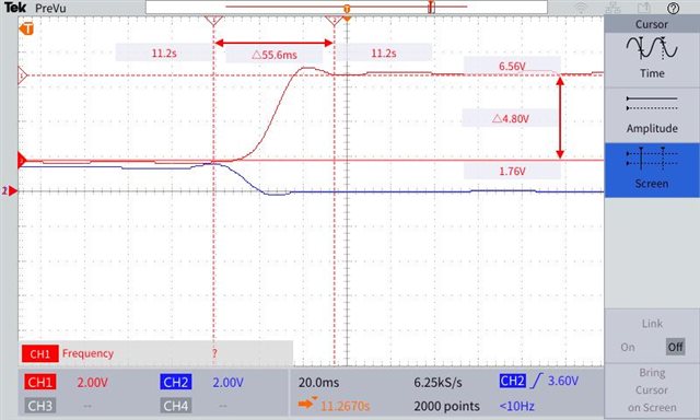
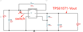
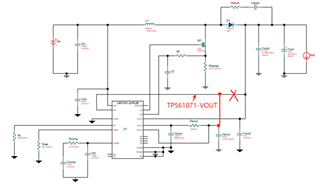
The waiting time from the start of the boost to the peak voltage is about 55.6ms after the switch is triggered. Our customer requested that this period of time be reduced to 30ms. How could to realize this? 

Thanks a lot!

Andy

  • Hello Andy,

    Thanks for reaching out to us via e2e.

    I am sorry, but you are not providing a lot of information, so I am guessing a lot here.
    I assume that the red signal is VOUT.
    What is the blue signal? Is it the Status pin?
    Why are you explicitly sowing the 1.76V level?

    What exactly do you mean when you say: "the switch is triggered"?

    Can you provide a schematic and a description of the test case?


    In general:
    This device is meant to keep the output stable while the input voltage breaks down to a low voltage.
    Therefore, it is powered by the VOUT pin (which is different from other controllers).

    This means that a booster which is based on this device CAN NOT properly start-up booting from a low input voltage (below 5.7V).

    The datasheet clearly states: Wide VIN input range from 1.5 V to 42 V - WHEN VOUT ≥ 5 V


    I assume that the input voltage in your setup is around 2.5V (so the output voltage is one diode drop lower which results in 1.76V).
    Then you expect the booster to start-up from there.
    Is that correct?

    When VOUT is 1.76V, the gate driver voltage will be even lower than that.
    You will hardly find any FET which can fully turn on with that gate voltage.
    Therefore, to provide a high enough gate voltage, the requirement is that VOUT has to be at least 5V to start the booster.

    If my understanding is wrong, the only thing you can do to speed-up the boost time is to increase the peak current by decreasing the current sense resistor.
    But please make sure that you will adopt the inductor and the FET accordingly.


    Best regards
    Harry

  • Hello Harry

    I assume that the red signal is VOUT.
    ——YES,The red line is the VMOT voltage signal of the LM51501-Q1

    What is the blue signal? Is it the Status pin?
    ——The blue line is the switching voltage signal.

    Why are you explicitly sowing the 1.76V level?
    ——Voltage 1.76V is the voltage value of VIN after passing through the diode, and LM51501-Q1 is not working at this time.

    Can you provide a schematic and a description of the test case?
    ——

    Input voltage VIN voltage is 1.8V-2.4V, output voltage VOUT voltage is 6.5V, using LM51501-Q1 chip.

    The blue switching voltage signal is controlled by the EN pin of the TPS61071 chip. After the EN high level is enabled, the VOUT output of the TPS61071 is set to 5.5V, and the VOUT of the TPS61071 is connected to the EN of the LM51501-Q1. The circuit diagram can be referred to the following picture:


    Best regards

    Jack

  • Hello Jack,

    Thanks for the additional information.

    Nevertheless, these Webbench diagrams do not really match with the customer's schematics.
    For examples, the resistor divider for the TPS61071 shows values for 3.3V, but you are stating that it is generating 5.5V.
    So, I do not know which other components have also been changed.

    Why has the LM51501 been selected for this application? It is meant for a different use case and is the wrong choice for this application.
    Feeding the VCC from an external source is not officially supported, so I can only warn that there might be a possible damage due to that.
    An external 5.5V voltage is basically driving against the internal regulator.
    Also, the datasheet clearly states that the device requires a minimum 5 V at the VOUT pin to start up which is violated here.

    As you already have the Aux voltage from the TPS61071, the correct device would be the LM5155.
    Dependent on the output power, the LM5157/58 may also be an option.

    Anyway,
    There is a QuickStart calculator for the LM51501 on our website which you can download from here:
    https://www.ti.com/lit/zip/snvc217

    Please enter 1.8V as an input voltage and you will see that an inductor of 2.3nH and a sense resistor of 6 Milliohm are recommended.
    If an inductor with 820nH is used, this will slow down the ramp.

    To reduce the overshoot you can also use the calculator for the compensation network.
    But please be aware that the parasitics of the board have a big influence and only experiments in the lab will allow you to find the right values that will slow-down the reaction time and eliminate the overshoot.


    All information in this correspondence and in any related correspondence is provided “AS IS” and “with all faults” and is subject to TI’s Important Notice (www.ti.com/.../important-notice.shtml).

    Best regards
    Harry

  • Hello Harry

    Use LM51501-Q1 chip.
    Under the conditions of input voltage 1.5V-2.4V and output voltage 6.5V@5A.
    According to the optimal design, the theoretical output voltage VOUT, from the start to the stable output of 6.5V, what is the minimum time?

    Best regards

    Jack

  • Hello Jack,

    I am sorry, I can olly repeat that this device is not meant for this type of application.
    Moreover, this device on its own cannot work with this input voltage range.
    So, the overall timing will always reflect a combination of both devices.
    This timing depends on the choice of the external components, so I cannot give you a number. I am sorry for that.

    As the customer is taking the overshoot into account, they can try to optimize / slow down the compensation to avoid the overshoot.
    Looking at the oscilloscope screenshot, this will buy them about 15 to 20 ms.
    They can also experiment with a smaller inductor and a smaller current sense resistor.

    All information in this correspondence and in any related correspondence is provided “AS IS” and “with all faults” and is subject to TI’s Important Notice (www.ti.com/.../important-notice.shtml).

    Best regards
    Harry