Because of the holidays, TI E2E™ design support forum responses will be delayed from Dec. 25 through Jan. 2. Thank you for your patience.

This thread has been locked.

If you have a related question, please click the "Ask a related question" button in the top right corner. The newly created question will be automatically linked to this question.

BQ76952: Current limiter circuit

Part Number: BQ76952
Other Parts Discussed in Thread: TIDA-010208

Tool/software:

Hello TI Team,

I'm using the BQ76952 as a slave in my BMS, and I want it to support my battery pack configuration. I am using 16 LFP batteries, each with a capacity of 100Ah and a voltage of 3.2V, to create a battery pack with a total voltage of 51.2V and a capacity of 5kWh.

Based on the high-side MOSFET design, could I use the TIDA-010208 reference design? Additionally, could you recommend a current limiter from Texas Instruments to add to my schematics?

Thank you for your assistance.

  • Hello Oussama,

    Yes, you should be able to use the TIDA-010208 Slight smile. You can share your final schematics with us if you want us to double check it.

    For current limiter, do you mean a pre-discharge type of circuit To avoid inrush currents on initial start-up? The BQ76952 has an integrated high-side P-FET pre-discharge and pre-charge drivers, which are used to limit the current of initial charge/discharge currents.

    Best Regards,

    Luis Hernandez Salomon

  • Oussama_BMS.pdf

    Hello Salomon,

    Thank you for helping me; I appreciate your assistance.

    I have attached my schematics and a similar BMS from the market. I understand that they use two coils and some chemical capacitors with 220 µF and 100 V. My goal is for my BMS to safely handle the high current from the 16 LFP batteries.

    Could you please review my schematics and provide any recommendations to ensure safety and reliability with the high current?

    Thank you for your support.

  • Hello Oussama,

    To safely handle high currents, you would have to design your board to do so, you would need your sense resistors and MOSFETs to handle the current.

    You seem to have already many FETs in parallel. I see you have two 2-mOhm sense resistors, will these be able to handle your current?

    As for additional comments on the schematic:

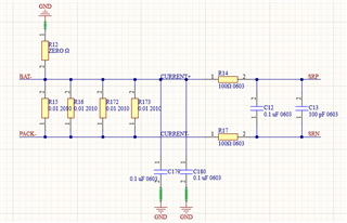
    • I'd suggest to add footprints for 0.1-uF capacitors on the SRP/SRN pins to Vss, just in case additional filtering is required.
    • R21 should be 20-Ohms for best accuracy on cell 16 during cell balancing
    • I'd suggest to make D38/D27 as do-not-place (DNP/DNI)
      • Only add if needed.

    Besides that, I think all looks good!

    Best Regards,

    Luis Hernandez Salomon

  • Hello Salomon,

    Thank you for your reply. Your assistance is very helpful, and I appreciate your time.

    I wanted to confirm my calculation for the voltage drop of 50 mV (0.05 V) at 100 A:

    R= 0.05V / 100 A = 0.0005 ohm

    This means I would need a shunt resistor with a value of 0.5 milliohms (0.0005 ohms).

    Power Rating of the Shunt Resistor:

    P= 0.05 V*100² A = 5 W

    • Shunt Resistor Value: 0.5 milliohms (0.0005 ohms)
    • Power Rating: 5 W

    Additionally, I have added a 0.1 µF capacitor to the ground on both SRN and SRP for filtering as shown in the capture bellow, which I believe is a good idea.

    I have a question regarding the number of parallel FETs needed to handle the current accurately. How can I determine this?

    Best regards, 

    Oussama.D

  • Hello Oussama,

    The power rating seems okay, but keep in mind that it should also need to be able to handle the worst-case conditions, such a short-circuit. You may want to contact your resistor provided to ask what are the pulse capabilities of the resistors. Or parallel more to handle the short burst of currents.

    Regarding the number of parallel FETs, that'd just depend on your expected current and how you want to manage the thermals of your MOSFETs. The more in parallel the more the heat would spread out and more current it would be able to handle.

    Let me know if you have more questions Slight smile.

    Best Regards,

    Luis Hernandez Salomon

  • Hello Salomon,

    I hope you're doing well.

    Could you please provide guidance on selecting an inrush current limiter or advise recommendation for a parallel battery pack setup (parallel BMS)?

    Thank you and have a great day.

    Best regards,
    Oussama D.

  • Hello Oussama,

    When paralleling BMS, you must ensure that the battery stack voltage is similar between the battery packs, otherwise there may be a high inrush current between the packs. Ideal diodes may be needed to control when the battery stacks are first connected.

    For a current limiting circuit, we have the pre-charge/pre-discharge FETs, which are really meant to control inrush currents due to capacitive loads, or to slowly charge the battery if needed.

    Best Regards,

    Luis Hernandez Salomon

  • Hello Salomon,

    Thank you for your prompt response. I would appreciate it if you could review the precharge section of my schematics to ensure everything is in order.

    Thank you for your assistance.

    I wish you a great day.

    Best regards,

    Oussama DallaliFET CHARGE AND DISCHARGE.pdf


    FET CHARGE AND DISCHARGE.pdf

  • Hello Oussama,

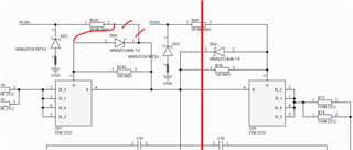
    I would actually recommend to not use the Zener diodes (D52/D25) here (At least make them DNI/DNP), also increase R243/R70 to 10-MOhm and decrease R242/R69 to 5-kOhm. I have seen this circuit perform better when those values are what I described.

    Also, it seems that the PCHG/PDSG pins are connecting to the source of the FETs. These both should connect to the Q51/Q20's gate node.

    Best Regards,

    Luis Hernandez Salomon

  • Hello Salomon,

    Thank you for your feedback. I've made all the changes you suggested, including adjusting the resistor values and marking the Zener diodes as DNI/DNP.

    However, I’m a bit unclear about your last point regarding the PCHG/PDSG pins. Could you please clarify the exact connection you’re recommending for these pins in relation to Q51/Q20's gate node?

    Thank you for your guidance.

    Best Regards,

    Oussama


    2605.FET CHARGE AND DISCHARGE.pdf

  • Hello Oussama,

    They look good there! Slight smile. I actually meant the following:

    Although it seems Q20 was correct there, but I see that you fixed Q51 in this new schematic.

    Best Regards,

    Luis Hernandez Salomon

  • Hello Salomon,

    Thank you for your support and assistance. Your guidance has been extremely helpful to me. Please accept my sincere respect.

    Best regards,
    Oussama

  • Oussama,

    Glad to help Slight smile.

    Let me know if you have any further questions.

    Best Regards,

    Luis Hernandez Salomon