


TI's gate drivers use a pull-up and pull-down structure in order to drive the output stage. The pull-up structure supplies the source current to turn on the power device, and the pull-down structure supplies the sink current to turn off the power device. Figure 1 shows the typical output stage of a gate driver:
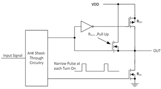
Figure 1: Example output stage of a gate driver with hybrid pull-up structure
Gate drivers require the output voltage to be within a safe level to prevent damage occurring to the output stage. Generally, the output voltage should not exceed VDD or go below GND (specifications are found in the Absolute Maximum Ratings section of the gate driver's datasheet). If the output experiences an overvoltage, the current could travel from the output pin to VDD through the body diodes of the pull-up structure. If the output experiences an undervoltage, the current could travel from GND to the output pin through the body diodes of the pull-down structure. High current flowing through these paths could cause electrical overstress and potentially damage the driver. Figure 2 shows a diagram of the path of current during an output overvoltage or undervoltage beyond the device’s specifications; the MOSFET body diodes are included as well:
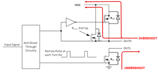
Figure 2: Current path during an output overvoltage or undervoltage event
In many cases, the output overvoltage or undervoltage is due to ringing caused by high dV/dt and dI/dt, which is created by parasitic inductances and capacitances paired with the fast switching of gate drivers. Proper PCB layout is important to limit parasitics (layout guidelines can be found in the gate driver’s datasheet). Other than layout, a simple solution would be to increase the gate resistance or place an external gate-source capacitor close to the device. Both solutions can damp the ringing by slowing down the rise/fall time. Figures 3 and 4 show the output signal of a gate driver with and without gate resistance, respectively:
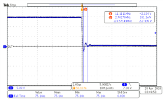
Figure 3: Output signal with no gate resistance
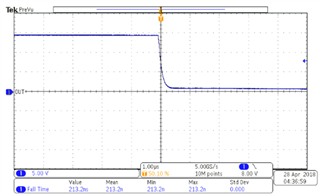
Figure 4: Output signal with gate resistance
Another solution would be to add diodes to the output pins. These diodes are used to clamp the output voltage from exceeding the forward voltage of the diodes, and they provide a path other than the internal body diodes for excess current to pass through. Schottky diodes are typically used, as they feature a very low forward voltage of about 0.3V. Fast forward recovery time is also another specification to consider when selecting the diodes.
Figure 5 shows a schematic of how the diodes are placed. Assuming both diodes have the same forward voltage (Vf), if the output voltage exceeds VDD + Vf, then D1 will turn on, and the excess current passes to VDD. If the output voltage is less than GND – Vf, then D2 will turn on, and the excess current passes to GND:
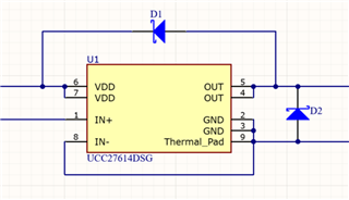
Figure 5: Output clamping diodes
Output voltage needs to be contained within the gate driver’s specifications, and exceeding the specifications may cause damage to the device. Proper layout, gate resistances, external CGS, and clamping diodes all help with reducing output overvoltage and undervoltage and avoid potential damage.
