LM5156-Q1: LM5156-Q1 DCM calculation tool

Part Number: LM5156-Q1
Other Parts Discussed in Thread: LM5156, UCC28600, TL431

Tool/software:

Hi Team,


Do you have LM5156-Q1 DCM calculation tool to calculate compensation values supporting multi-outputs?


LM5156-Q1 DCM desgin tool was discussed in e2e below.

https://e2e.ti.com/support/power-management-group/power-management/f/power-management-forum/1290003/lm5156-dcm-design-tool?tisearch=e2e-sitesearch&keymatch=LM5156%20AND%20DCM#


As discussed in it, https://www.ti.com/tool/download/SNVC240 is only for CCM designs.

Also I cannot select LM5156 in https://www.ti.com/tool/download/FLYBUCK-FLYBACK-DESIGN-CALC.


Regards,

Kai

  • Hi Kai,

    Thanks for reaching out.

    Unfortunately we do not have a tool to calculate the compensation in DCM.

    However, if the compensation is adjusted for CCM it is normally also stable in DCM.

    There is an appnote about isolated compensation design using a TL431 with UCC28600: https://www.ti.com/lit/an/slua671/slua671.pdf

    There you can find explanations for hand- calculations of the compensation components in DCM.

    If you have firther questions, please feel free to ask.

    Best regards

    Moritz

  • Hi Mortiz,

    I am revisiting for help.

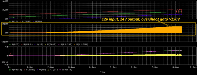
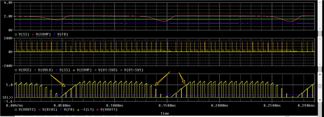
    I have run the Pspice for TI using flyback for 900V input using case. And found 2 abnormal waveforms. Can you kindly provide your professional help?

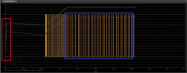
    1, Why red box here, will have a sharp rising of output, before SS starts?

    2, Why blue box here will have hiccup gate signals? The file I used is LM5156.

    BRs,

    Marsh

  • Hi Marsh,

    Can you please provide the schematic you are simulating and the specs (Vin Vout Iout)?

    Thanks and best regards

    Moritz

  • Hi Moritz,

    Thanks for the reply.

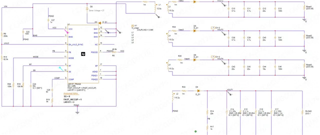
    1, Here is the simulation sch.

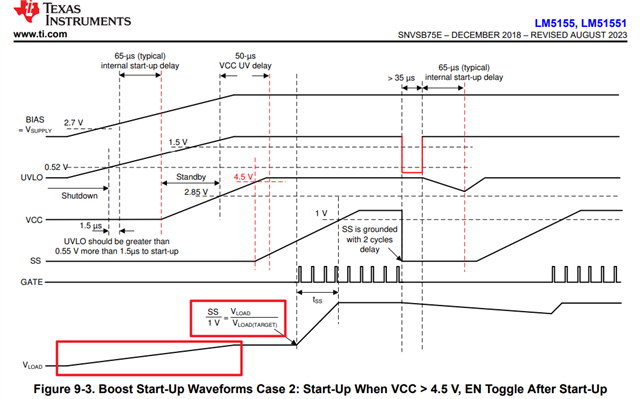
    2, Can you kindly explain the red box waveform ? Why before the device startup, the output will have a voltage = Vload(target)*SS/1. We are assuming that what we are seeing at the simulation(original post) is resulted from here. What's the root cause of this voltage? How to prevent this or make this voltage small?

    BRs,

    Marsh

  • Hi Marsh,

    Can you please provide the specs for your simulation file?

    What is the Vin, the Vout for the different rails and the Iout?

    Maybe you can also provide your simulation file.

    Regarding the softstart waveform, the picture in the datasheet is for boost topology. For a flyback this waveform would be different as the output voltage will start from 0.

    The ramp in the red box comes from the fact that there is a natural pass through path from the input to the output because of the rectifier diode.

    Best regards

    Moritz

  • LM5157_PSPICE_TRANS.7z

    Hi Moritz,

    Thank you for the reply.

    Please kindly find the attachments for calculator (design requirements) and simulation file. Please kindly help to modify the simulation file to make it match the calculator. Thanks.

    Support need and issue description:

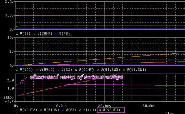
    1, Abnormal output (out1) ramp. I have set IC of the caps to 0. But the ramp is still there. Please kindly check the root cause.

    2, RCD snubber tuning. The overshoot are too large.

    3, Most important, loop tuning. Seems sub-harmonic oscillation appeared after ss.


    BRs,

    Marsh

  • Hi Marsh,

    LM5157_PSPICE_TRANS_fixed.7z

    1. Setting 0V as IC for output caps removed the ramp in the beginning.

    2. The overshoot is reduced by picking a turns ratio of 1:3 instead of 1:9. Also RCD clamp was improved.

    3. The oscillations were removed by increasing output capacitance and improving compensation.

    Best regards

    Moritz