This thread has been locked.

If you have a related question, please click the "Ask a related question" button in the top right corner. The newly created question will be automatically linked to this question.

TPSM33615: Using SW node from

Part Number: TPSM33615
Other Parts Discussed in Thread: TPSM33625, TPS62810,

Tool/software:

Hello,

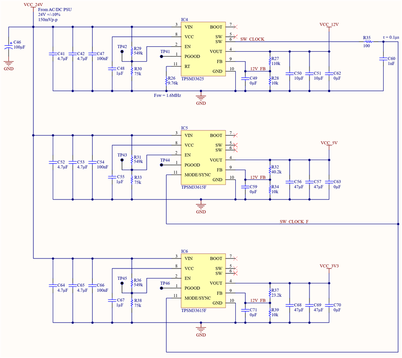
The TI Application Note "Different Strategies for Synchronization" (SLVAEG8) gives a number of different strategies for synchronising clocks in multiple buck converters. I would like to use the strategy described under "1.4 Synchronization to the Other DC/DC Converter", where the principle is to use the SW node from one buck converter as a clock source for others. Thereby ensuring predictable, out-of-phase synchronisation. I have chosen the TPSM33625 for the "master" buck converter, and TPSM33615F for two "slave" buck converters, as shown in the overview below (no external components shown):

Current requirements of each power rail:

- VCC_12V: 1.5A (constant)
- VCC_5V0: 1.3 A (audio amp supply, normally very low-load, with occasional peaks to max. load)
- VCC_3V3: 1.1A (constant)

Simplicity and EM noise control are both important in this design, which perhaps helps to explain some of the design decisions. I'll be sure to respect the layout guidelines in the datasheet when I get to that.

I have a few questions about this:

  1. The application note actually uses the TPS62810 in the example, and says that "TPS62810 synchronization is designed in a way that the switching is out of phase". Is this approach also supported by the TPSM336* family in the way it's wired up above?
  2. I chose 1.6MHz as the switching frequency using Table 7.1 in the datasheet. By forcing the 5.0V power rail to switch at 1.6MHz, even when operating under very light load conditions, is it correctly understood that the TPSM33615F device will be operating in FPWM mode? (i.e. With reverse current through the inductor?)
  3. Assuming my calculation are correct, the minimum on time should be respected, so would it be correct to assume that the device will not enter Valley Current Mode Operation (and any noise unpredictability that may result from that)?
  4. Is clocking the TPSM33615F at 1.6MHz under very low-load conditions supported indefinitely? Is there any way to estimate the wasted power?

Many thanks for any help offered.

Best regards,

Eddie

  • Apologies, I seem to have accidentally chopped off the full-length title. I had intended it to read: "Using SW node from a buck-converter as an out-of-phase clock source for others."

  • Hi Edward,

    Thank you for your questions. I believe your schematic is having trouble loading. Regardless I believe I am still able to address your questions.

    1.The Mode/Sync pin for this device has an ABS MAX rating of 5.5 V, which the SW node will exceed. This is not a recommended use case for this device and may cause damage to the subsequent devices. I also imagine that the trace from SW required to accomplish this synchronization would harm EMI performance. 

    2. If minimum-on-time is respected, then the part will not operate in Valley Current Mode.

    3. Low-load conditions in FPWM will have low efficiency due to the reverse current that flows through the inductor increasing your switching losses. The Webench model for this device should provide a good way of estimating the power losses associated with this usage case.

    If you have any more questions, please feel free to reach out,

    Thank you,

    Joshua Austria

  • Thanks Joshua. I'm not sure why the schematic didn't load properly. I'll try uploading it again here:

    1. Good point about the abs. max limit on the MODE/SYNC pin. I suppose if I wanted to make it work as shown above, then I could use the 3.3V converter as my "master" clock source instead. However, that would entail having the 12V and 5V rails synced in-phase with each other, which would be a little unbalanced. Therefore I would probably prefer to buffer the 12V clock source with an n-channel MOSFET or the like. With that in mind:
      1. Could you tell me the approximate input impedance on the MODE/SYNC pin?
      2. Could you tell me the logical relationship between a high signal on the MODE/SYNC pin, and the voltage at the SW node? (In the app. note I referred to, it appeared to be an inverted relationship.)
      3. Is there anything about my proposal to translate the 12V clock "source" that might give you cause for concern? 
    2. Many thanks for confirming this.
    3. Unfortunately I couldn't get the Webench Power Designer tool to work at low currents (0.01A in this case). Neither by starting with a high-current (which worked fine) and then reducing it (which caused a "Design Update Failed" error), nor my starting a new design from scratch with a low current (which caused a "Design cannot be created!" error).
  • Hi Edward,

    I don't believe the input impedance is measured with this part nor is the logical relationship with MODE/SYNC and voltage at SW, but I can test this.

    However, my advice is that siphoning the SW signal for this device is not tested and may result in abnormal waveforms/regulation. The SW node itself is not really meant to provide a driving signal, so you could interfere with the operation of the device. TI recommends an external clock source be utilized for the Mode/Sync for this part.

    I will note, that we do have parts such as the LMQ644A2-Q1 that offer a "SYNCOUT" pin for applications such as these. This pin can be used to synchronize subsequent devices to the switching frequency of a singular IC.

    Thank you,

    Joshua Austria

  • Hi Joshua,

    Thanks a lot for your reply. I'm sorry to hear that TI doesn't recommend the synchronisation setup in my circuit diagram. Would you be able to say specifically what is it that's different here, in comparison to the setup described in the TI application note SLVAEG8 (section 1.4)? TI seems to be selling the solution very convincingly there.

    I did consider using a multiphase clock source (e.g. LTC6902) but when I saw that application note I really liked the simplicity of it, not to mention the LTC6902 is rather expensive.

    If I were to design-in the possibility of this synchronisation, and were to find that all waveforms looks as expected (i.e. they look similar to when they are driver by an external clock), would that be a sufficient verification? Or are the types of problems you imagined too spontaneous to be sure of catching them in a single scope reading?

    If you have an eval board and scope to hand, and are as curious as I am to know if this would work, then I would be very grateful to know the relationship between MODE/SYNC and the SW pin.

    Best regards,

    Eddie

  • Hi Eddie, 

    Apologies, I will be a little more clear. I cannot say that this device (TPSM33615) will work with this application as it remains un-tested. The application works in that application note specifically for the TPS62810, but this is not to say that it will work with all DC/DC converters. There could be any number of differences between the parts that would jeopardize the application. For example, that part in particular is a low voltage part, and it could be the case that at higher voltages, the SW node would be more sensitive than the part in the application note and cause the TPSM33615 to malfunction. In any case, the datasheet in figure 5-1 does not recommend placing any external component on the SW pin or attaching it to any signal. I have included this section below for your convenience:

    With all of this being said, as long as the absolute maximum ratings of the part are considered, I would not be surprised to see it work, given the app note. If you were to design the application, and the waveforms are as expected, then you would be all set. I would take tests at varying loads to confirm the application's function.

    All TI can confirm is that in a vacuum, the TPSM33615 can synchronize it's switching frequency to an external signal and that it's SW pin is not designed to output a signal. I wish you well on your endeavors and hope TI can support your application.

    Thank you,

    Joshua Austria

  • Hi Joshua,

    Yes, I agree that looks pretty clear. Thanks a lot for your support!

    Best regards,

    Eddie