- Ask a related questionWhat is a related question?A related question is a question created from another question. When the related question is created, it will be automatically linked to the original question.
This thread has been locked.
If you have a related question, please click the "Ask a related question" button in the top right corner. The newly created question will be automatically linked to this question.
Tool/software:
Hello Ti,
Please check below the Schematic Attached, we are unable to get the desired outputs from the Output rails of this IC. The Schematic is designed by referring to TPS65216 PMIC Datasheet.
Hello Hatim,
It may be difficult to determine the exact reason that you are not getting the desired output values,
Are you able to provide any scope captures to show what output levels you are getting from the rails?
Additionally could you provide the register readings, and check registers 0x01 and 0x02 for any fault flags?
Regarding the schematic,
can you provide the values of the output capacitors for each DCDC ?
And I notice that there is an extra inductor (L32) at the DCDC4 pin. May I ask the purpose of adding this component?
Thank you,
Sarah
Hello Sarah,
Que: Are you able to provide any scope captures to show what output levels you are getting from the rails?
Answer: No, We are not getting any output from DCDC rails, all the input pins of DCDC rails are supplied by 5V.
Que: Additionally could you provide the register readings, and check registers 0x01 and 0x02 for any fault flags?
Answer: No, I think IC isn't turning on so unable to check the registers 0x01 and 0x02 via I2C.
Que: can you provide the values of the output capacitors for each DCDC ?
Answer: yes, I have attached the Spreadsheet for the passive values.
Que: And I notice that there is an extra inductor (L32) at the DCDC4 pin. May I ask the purpose of adding this component?
Answer: Yes, it was a mistake from our side we removed the inductor and short the inductor pads.
Hi Hatim,
LDO1 is set to output 1.8V by default for the TPS65216? Can you connect input voltage and add output capacitor to LDO1?
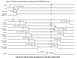
LDO1 should enable as soon as a WAKEUP event is triggered and the enable delay time has passed. LDO1 is usually used as the pull-up voltage for nWAKEUP and nINT since it is the first rail to power up after a WAKEUP event.
Using DCDC4 means that you will not have a proper pull-up source until later in the sequence which is not ideal.
Regards,
James
Hello James,
We are not using LDO iit is NC in our circuit, also for testing purpose we supplied external 1V8 pullup at nWAKEUP and nINT pins. Still no output is obtained.
Hi Hatim,
We need to see scope captures of your input voltage ramp up and digital signals otherwise analysis will be difficult.
Please share a capture of IN_BIAS, nWAKEUP, PWR_EN, and nINT as a start.
LDO1 is enabled by default on this device so you may be encountering a power fault as LDO1 tries to enable but is missing external components. One thing you can try is supplying the IN_LDO1 pin with your 5V source to see if that allows for proper power up. The pin description in the datasheet for LDO1 output indicates that an output capacitor is needed so that LDO1 can reach power good and a fault will not be triggered.

Regards,
James
Hello James,
Thankyou for your help, we gave the External 5V supply to the IN_LDO1 pin and the PMIC got turned ON.
I have one more question regarding the Active state of the PMIC, In a datasheet the PB pin is supposed to be pulled up first and then connected to the push button. But we don't want a push button on our PCB board as we are using this IC for a non portable device, so what must be the condition needed to be implemented that after Turning ON main 5V supply to the PMIC , it must be in active state or in permanant ON state unless and untill the main supply is turned OFF.
Hello James,
DCDC1 and DCDC2 generate a default output of 1.1V and both be adjusted via I2C (According to the Datasheet).
Can we connect an external feedback circuit to the FB2 pin of DCDC2 to produce 1.2V for my DDR4 memory instead of using I2C for the adjustment?
Hi Hatim,
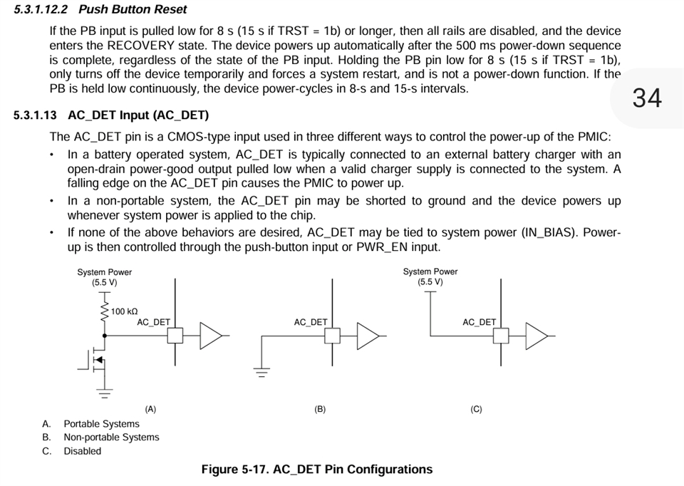
For the PB pin, if you are not using a push button, you should be able to leave this pin floating. The PB pin has an internal pull-up resistor (100k) to your SYS voltage so if the pin is left floating you should not see any interference in ACTIVE state.
You can add a FB resistor divider to adjust the buck output to 1.2V. I would recommend using at least 1% tolerance resistors for better output accuracy.
Regards,
James