This thread has been locked.

If you have a related question, please click the "Ask a related question" button in the top right corner. The newly created question will be automatically linked to this question.

TPS53119: TPS53119 review schematic

Part Number: TPS53119

Tool/software:

hi,

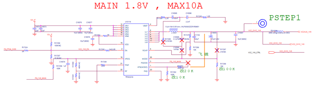
The schematic diagram of TPS53119 is shown below, with an input voltage of 12V, an output voltage of 1.8V, and a maximum output current of 10A. Please help check if there are any issues with the schematic diagram. Thank you!

  •  

    Thank you for using TI and for reaching out for assistance.

    There seems to be some edits made to the schematic, I will comment on those edits.

    1) It appears the RCC injection circuit across L10007 has been removed.  The TPS53119 uses D-CAP mode control.  D-CAP mode control requires output voltage ripple in-phase with switch timing to regulate and stabilize the output and switching frequency.  The output capacitance appears to be made from 1x 2.5V 470μF electrolytic capacitor in parallel with 1x 100μF and 1x 10μF ceramic capacitors.  I am concerned they will not provide enough output ripple at the right phase shift for the control loop.

    With the floating RF pin, the nominal switching frequency is 500kHz, and the 1.5μH inductor will have 2A peak to peak ripple.  To have a minimum of 10mV ripple at FB, the converter would need 30mV of output voltage ripple, for a minimum ESR of 15mΩ.  Unfortunately, even if the 470μF capacitor has 15mΩ of ESR, the 100μF capacitor will start to reduce the impedance at 100kHz and the ripple will not be at the correct phase.

    If the 470μF capacitor has 15mOhms or more ESR and you can tolerate 30mV of output ripple, remove C11102.  Otherwise, you will need to populate the RCC injection across the inductor.

    In order to get 10mV of ripple at the FB pin, you'll want an R-C time constant between R17266 and C16598 of 300μs, so you can populate R17266 = 3.01 and C16598 = 0.1μF

    You'll need C16599 to inject the ripple into FB, but it needs to be into the VFB pin (Pin 1), not the MODE pin (Pin 20).

    The added ripple will raise the average voltage at VFB to 0.605, so you may want to adjust R17263 (decrease) or R17262 (Increase) about 1% to adjust the output voltage, or Vout will be 1.815V

    2) The ROVP pin should be connected to VOUT with the same resistor divider ratio as the VFB, so populate R17270 with 20kΩ

    3) 100μF and 10μF ceramic capacitors tend to introduce an "inter-capacitance resonance" when used in parallel.  You may want to consider increasing C16597 to 22μF to prevent a noise spur at 1.5MHz.

    Due to the number of edits in the schematic, can you share your schematic after you have updated it so we can verify that the connections have ben made correctly?