Other Parts Discussed in Thread: TLV4051
Tool/software:
Dear TI support team,
I'm developing the power management for a long life battery powered small device. The device operates most of the time in low power mode, when current consumption is below 50uA, so low quiescent current is essential. The input voltage of the device can be either 3.6V, 6V or 7.2V (depending on what battery configuration used), with highest ripple of 0.5V at heavy peak loads. The output voltage can be in the range of 3.3-3.8V, but want to keep at lower end for better power consumption reasons, at 3.3V. Iout max: 2A
We have found TPS62902 buck converter for this task is the most suitable and ordered the evaluation board to validate it. The IC passed all of our requierements, except one: the IC can't work in power save mode, when Vin =3.6V, and Vout = 3.3V. This is stated in datasheet: " When VIN decreases to typically 15% above VOUT, the TPS62902 does not enter power save mode, regardless of the load current." So my idea was to add a little external circuitry to be able to bypass the buck converter when input voltage is below 3.8V. Note that the available footprint is very limited, my designs on the edge. I've tried multiple concepts, but failed so far, that's why I'm asking for reviews/solutions.
- Make Vout software adjustable to 3.3V or 3.7V, by switching the resistor divider. So at 3.6V configuration the buck converter will work in 100% duty-cycle mode.
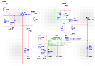
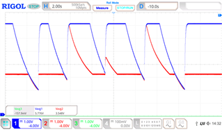
Switching the resistor divider at runtime worked well, but the 100% duty-cycle mode consumes almost 1mA, which is not acceptable for our usecase. - Make use of the precise enable (En), and PG pins, and if PG stays low a bypass MOSFET is switched externaly. You can see my schematic at the attachments, I also had to add a delay network, because PG needs about 2ms after power on. This solution almost worked, but due to the delays and capacitive elements it can bypass higher voltages when switching Vin at good timing, like when inserting the battery. See my measurement at the scope picture. Ch1: Vin, Ch2: Vout
- Have a comparator which switches either the buck converter or MOSFET.
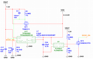
As I looked for comparators I've found that either I have 7.2V tolerant IOs but have to add external voltage reference, or have internal voltage reference but the IOs are not 7.2V tolerant. I went with the former and found TLV4051 family. My concept was at power-up the buck converter starts switching, and from Vout it powers the comparator, which will switch to bypass mode if the Vin voltage is too low. I could not test this connection as I don't have the comparator at the moment, but I think the previous power on switching issue can still occur.
So my questions:
- What do you think about my #3 design? Does it seem working, or still has the power on switching issue?
- Can you reccommend a working concept or connection for this purpose?
- Is there other buck converter which would be better for this task? Which has low Iq and have bypass mode in the package?
Best regards,
Peter