This thread has been locked.

If you have a related question, please click the "Ask a related question" button in the top right corner. The newly created question will be automatically linked to this question.

TPS65219: TPS6521903RHBR No power output

Part Number: TPS65219
Other Parts Discussed in Thread: TLV62595, ,

Tool/software:

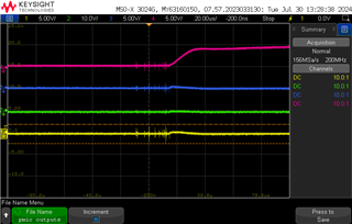
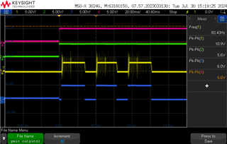
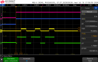
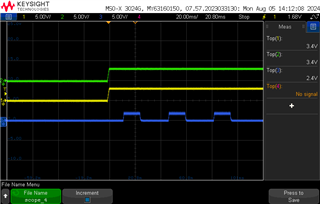
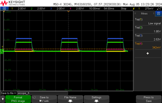
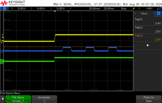
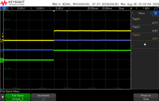
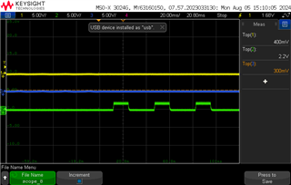
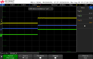
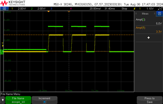
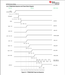
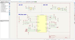
Hello, I recently designed the AM6254 based processor board with the TPS6521903RHBR PMIC, when I Power on the board the 3.3V buck convertor turns on for few ms then remains off after that. sharing. it looks like PMIC GPO2 pin pulls down the LDO enable PIN.

I have also replaced the PMIC from the market purchased board and swap it with the Newly designed board. The market board works well and getting all the outputs from the PMIC but not getting from Newly designed board.

The 3.3V Buck convertor is TLV62595DMQR. (DCDC_3V3)

Thanks and Regards

Mohit 

  • Hi,

    Thanks for reaching out. Could you provide more information on the differences between "market purchased board" vs "newly designed board"?

    Additionally, could you provide the PMIC schematic in a searchable PDF so we can perform a review?

    Thanks,

    Brenda

  • Market purchased board is the BeaglePlay (https://www.beagleboard.org/boards/beagleplay) and Newly designed board is the same board I designed with the schematic available (https://git.beagleboard.org/beagleplay/beagleplay).

    Attaching the PDF format for the PMICPlay-SoC GPIO 3.3V.pdfPlay-DC_DC AND PMIC.pdf

  • Thanks for sharing the schematic! The internal parameters for the buck converters are optimized for 0.47uH inductor. Could you change the inductor on Buck1 from 0.33uH to 0.47uH?

    After the Buck1 inductor is changed. Could you also share a scope capture with the following signals:

    • VSYS
    • BUCK2
    • LDO3
    • BUCK3

    Thanks,

    Brenda

  • I had changed the 0.33uH inductor with the 0.47uH inductor and below is the outputs of the PMIC.

    Pink represents VSYS

    Blue Represents Buck3(Pin 27)

    Green represents BUCK2(Pin 29) 

    Yellow represents LDO3(Pin 21)


  • Additionally will be sending you one more waveform 

    Pink represents VSYS

    Green represents Enable

    Yellow represents TLV62595 Buck convertor (pin 5 output)

    Blue Represents GPO2

  • Hi,

    The last scope capture shows significant noise coming from the external TLV62595 Buck. Could you disconnect the load from all PMIC rails and isolate the power solution?

    Thanks,

    Brenda

  • Hello,

    I tested  with the no load condition the results are same.

  • Additionally I had also testing the sequence again, 

    Pink represents VSYS

    Blue represents Enable

    Yellow represents GPO2

    Green Represents buck 2 output after inductor.

  • If the green channel is Buck2, does that mean you are getting 5V on Buck2 when it tries to turn ON?

    Thanks,

    Brenda

  • sorry, GPO2 is green and buck 2 output is yellow. Please let me know the root cause 

    thanks

    Mohit

  • Do I have to configure it first from the TPS65219 GUI from TPS65219EVM-SKT to turn on the Buck outputs.

     I have also tested the same TPS6521903RHBR IC to solder directly to beagleplay board and it shows me the output of every buck and LDO's outputs as mentioned. So from this I think that it doesn't need preprogramming for using.

    thanks 

    Mohit

  • Hi,

    TPS6521903 comes pre-programmed from factory so it doesn't require NVM programming. 

    From the scope captures we have received so far, it seems like GPO2 as well as Buck2 are turning-ON for a period of time. Could you provide a similar power-up scope capture for the remaining PMIC rails to see if they turn-ON for a period of time?

    Do you know why the external 3.3V Buck (TLV62595) has so much noise at the output? I'm suspecting this could be affecting LDO1, LDO3 and LDO4 because these LDOs are supplied by the external Buck. 

    Thanks,

    Brenda

  • I have supplied 3.3V from external souce not from TLV62595. For the above testing. 

    Thanks

    Mohit

  • Hi,

    I am also getting a voltage of 1.8V at VDD1P8.

    Additionally. I feel like there could be some error in the Schematic. Please review the schematic and please let me know the minimum circuitry to run the Buck2 output (1.8V) and then remaining buck and LDO outputs

    Thanks

    Mohit

  • Hi Mohit,

    What is the sequencing of the external supply that was used to supply the LDOs? Does it turn-ON at the exact same time as VSYS? Could you provide a scope captures of VSYS, the external supply of the LDOs and all the PMIC output voltages (Bucks and LDOs)?

    Thanks,

    Brenda

  • Below are the waveforms listed as follows -

    Green - PVINLDO1

    Blue - PVINLDO2

    Yellow - PVINLDO34

    Green - VLDO1

    Blue - VLDO2

    Yellow - VLDO4

    Green - VDD1P8

    Blue - VLDO3

    Yellow - 3.3V out from TLV62595

    Green - PVIN_B2

    Blue - PVIN_B3

    Yellow -PVIN_B1


    Green - LX_B2 after inductor

    Blue - LX_B3 after inductor

    Yellow - LX_B1 after inductor

    Green - EN

    Blue - Mode/Reset

    Yellow - GPO2

  • Hi Mohit,

    Could you provide a picture of the PMIC IC top marking? I'm staring to think you don't have the correct orderable or the channel labels were not identified correctly because I dont see the correct output voltages, sequence and one of the PMIC rails (GPO2) seem to be excluded from the power-up attempts. Here are a few observations:

    Green - VLDO1

    Blue - VLDO2

    Yellow - VLDO4

    • When LDO1 turns-ON, it only outputs around 1.6V-1.8V but the output voltage of this rail is controlled by the VSEL digital pin. If VSEL is high, LDO1 should output 3.3V.
    • Similarly, LDO2 does not have the correct output voltage. TPS6521903 has LDO2 configured to output 0.85V but your scope capture is showing approximately 2.4V. What do you have on channel 4?
    • LDO1 and LDO2 are turning-ON at the same time in your scope capture but the TPS6521903 was configured to turn-ON LDO2 6ms after LDO1.


    Green - EN

    Blue - Mode/Reset

    Yellow - GPO2

    • In this capture, I dont see GPO2 going low and high. The PMIC was design to execute a cold reset if an issue is detected in any of the PMIC rails. Your scope captures show some of the PMIC rails like Buck2, LDO1, LDO2 going low and high (3 attempts) but GPO2 seem to always stay ON. PMIC does not do this.

    Did you copy the same exact schematic and layout from the BeaglePlay board? Any schematic or layout differences? Have you try re-placing the PMIC with a new one and also trying on a new PCB? Are you able to completely isolate the PMIC by desoldering any load or external ICs connected to the outputs?

    Thanks,

    Brenda

  • Hi Brenda,

     I will be sharing the photo of the IC that was soldered and also I have made several iterations with no load condition, and the output waveforms remain same. I forgot to tell you the Output of GPO2 is remains high because I was directly pull up the pin by 0ohm resistance instead of 10K as mentioned. Refer to the schematic Resistor R2.


    After now I again put it 10K resistance on R2 and then I am getting the below waveform.

    Green represents GPO2

    yellow represents output of TLV62595.

    After connecting 10K in place of 0R (R2) the output of BUCK U2 is also not turning ON because the GPO2 is directly connected to the enable pin of TLV62595.

    I had copied the Exact same schematic . For layout considerations I have followed the Datasheet of the PMIC not the beagleplay board layout.

    I had also tested by placing my ordered PMIC on the beagleplay and beagleplay PMIC on my board. But it doesn't work. The beagleplay works fine but having the same issue with our board.

    By the way I figured it out that the beagleplay preinstalled IC is PTPS652193 is it same as TPS6521903RHBR.But as mentioned in the Schematic and documentation they have used TPS6521903RHBR as mentioned in their BOM.

    Yes I had made 2 board with the exact no load conditions, with only PMIC and TLV62595 BUCK.

    Please let me know if their are differences in PTPS652193 and TPS6521903RHBR

  • Thanks for sharing an update. We will review and provide feedback within the next 24-48Hrs.

    Thanks,

    Brenda

  • Hi,

    Brenda

    Please update on this.

    thanks 

    Mohit

  • Hi Mohit,

    "TPS652193" is not an active device in our portfolio. BeaglePlay uses TPS6521903. I'm wondering if there were any differences in your schematic compared to the Beagle board. It seemed very similar but it wasn't an exact copy because at least the Buck1 inductor was different.   

    Have you done a detail visual inspection of the soldering in your PCB? From the picture that was shared we can identify multiple areas of improvements from solder joints that are not clean.. The Buck1 inductor seem pretty big in size and the output caps from all Bucks do not seem to be installed. The 2 boards you mentioned in your previous message, do they only have PMIC and external Buck? no other ICs/load at all (including the VTT rail for the DDR)?

    Could you share the PMIC layout in a .brd file or Altium file?

    Thanks,

    Brenda

  • Hi

    Brenda,

    I have done the detail visual inspection of the board. I think so not installing the output caps will result in shut down of PMIC. The 2 boards I have said have PMIC and the 3.3V buck convertor. I have designed this project in KiCAD software as its not the Altium file so I will be sharing you the Gerber of that whole board. 

    Additionally I think that there are some issues the layout as FBx pins are connecting to the zones instead of connecting with the traces. I had tested with connecting the PMIC outputs of beagleplay of all Buck and LDO's to my board with every load connected and PMIC unsoldered on my board. Encountered the same issue with after some ms the 3.3V shuts down. Then I unsoldered all the wires and test it with only attached the 3.3V and then when I was connecting the 1.8V buck the PMIC shuts down.

    I will also be attaching the whole project folder

    Play.zip

    GERBER_BEAGLEPLAY.zip

    Thanks 

    Mohit

  • hi Brenda, 

    Can I know the dependency for turning On the GPO2 and 1V8(Buck2) voltage according to the schematic what are the important components that need to be soldered. 

    Need minimum number of circuitry and will do the testing in phases.

    Thanks Mohit

  • Hi Mohit,

    To test the minimum circuitry for the PMIC, you just need to completely disconnect the PMIC load from all Bucks and LDOs. For Bucks, you just need to keep the input/output caps and inductor.

    Thanks,

    Brenda

  • Hi Brenda, Can I know the dependency for the GPO2 pin which tries 3 times to pull up, ACC to power sequence first GPO2 will be ONN the remaining Bucks and LDO will be ONN.

    thanks 

    Mohit

  • Hi Mohit,

    Can I know the dependency for the GPO2 pin

    Could yo clarify this question? What do yo mean by "dependency"? GPO2 is configured to be part of the power-up/power-down sequence. If the device detects a fault in any of its rails, it executes a COLD reset on all DCDCs, LDOs and GPOs. 

    Thanks,

    Brenda

  • Hi Brenda,

    Please let me know if there are issues related to layouting.

    Thanks and regards 

    Mohit

  • Hi Mohit,

    I was able to import the KiCAD layout file to Altium which allowed me to review the routing for the main components (input/output caps and inductors). Please find my feedback below and let us know if there are any questions.

    • The routing for all the feedback pins (FB_Bx) does not match our layout guidelines. The FB_Bx pins must be routed as a trace directly from the local output cap to the corresponding FB_Bx pins. 
    • R9 and R10 are not needed. 
    • Do not connect the AGND pin (#15) directly to the thermal pad. As noted in the datasheet layout guidelines, this pin must be connected directly to the ground layer with a VIA. 

    Thanks,

    Brenda