Other Parts Discussed in Thread: TPS51285A, , CSD17302Q5A
Tool/software:
Hi team,
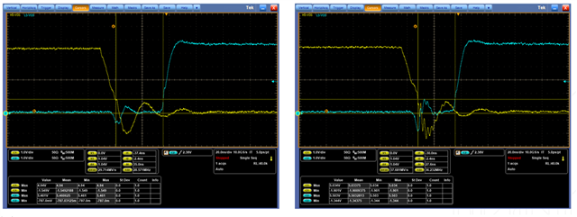
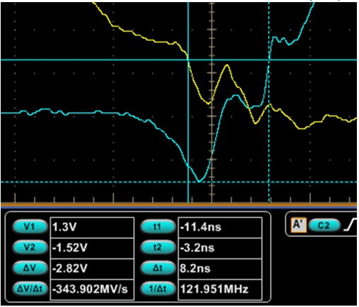
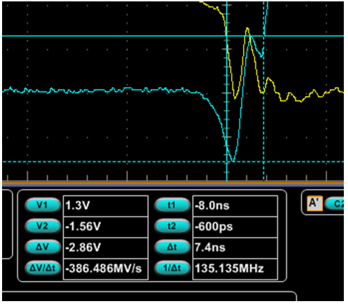
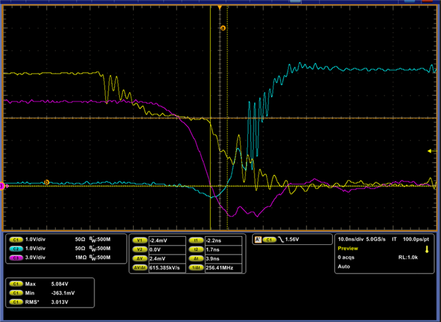
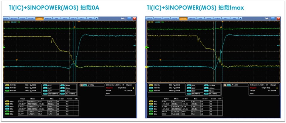
customer want their switching deadtime could be larger than 10nS spec,
I know it's related to MOS Qg as well, but since it's fixed.
is there any workaround we can do on the schematic on snubber value?
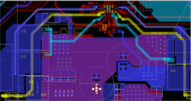
schematic above: