This thread has been locked.
If you have a related question, please click the "Ask a related question" button in the top right corner. The newly created question will be automatically linked to this question.
Tool/software:
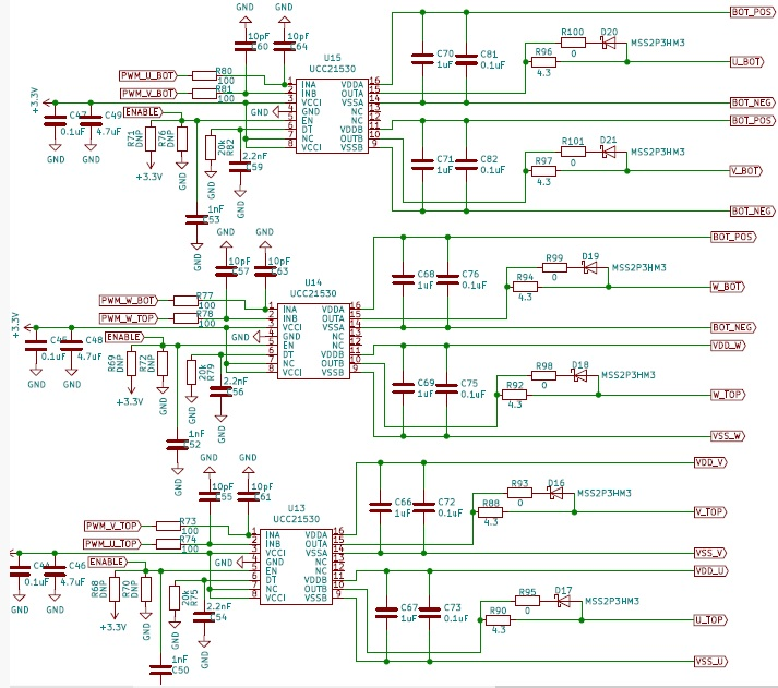
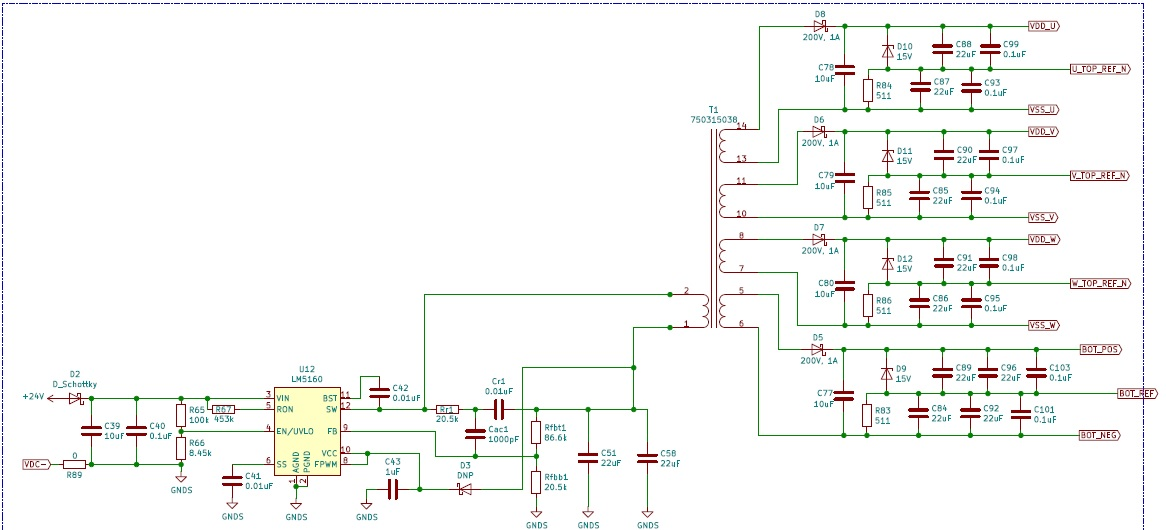
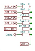
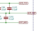
I have designed a 3 phase inverter using the UCC21530 drivers. The drivers are powered by an isolated bi-polar power supply similar to TIDA-00199. Power supply outputs are +15VDC and -8VDC relative to a reference that is tied to each high side output leg. The same outputs are also tied to a common -VDC low side reference. The configuration to drive the IGBT module are as follows:
1) UCC21530 Driver #1 - Low Side U, Low Side V
2) UCC21530 Driver #2 - Low Side W, High Side W
3) UCC21530 Driver #3 - High Side V, High Side U
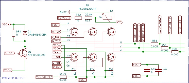
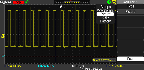
The output on Driver #2 appears as I would expect. The 0 to +3.3V PWM signal from the microcontroller is amplified to +15V and -8V on the VGS pin of the IGBT module for both the Low Side W and High Side W.
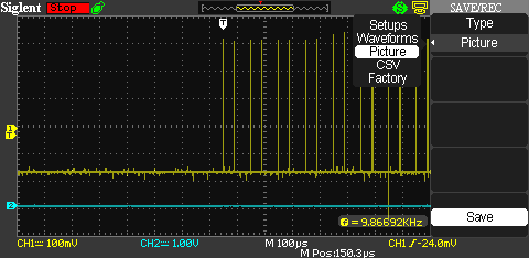
The output on Driver #1 and Driver #3 seems to truncate most of the signal or not generate any signal for both the Low and High side U, and V legs.
I have tried replacing the drivers, swapping them around, removing the IGBT module from the circuit. I always end up with Driver #2 working properly and Driver #1 and #3 truncating most of the output signal. The only conclusion that I can draw is that Driver #2 works because it's amplifying a Low Side and a High Side signal whereas Driver #1 and #3 are both amplifying either a Low Side or a High Side signal.
Does anybody have an idea why I can't generate the proper output signal on Driver #1 and Driver #3?
Regards,
Hi StnGgC,
Are you able to measure the Vdd-Vss power supply voltage across all of the channels? Also, can you share your schematic?
All the output channels should be isolated, and it should not matter that one has both a high-side and low-side. Unless that affects they way you have connected the power supply.
Also, you should try using UCC21551 which is an updated device that is more resistant to damage.
Best regards,
Sean
Sean,
Yes, I measured 25V across Vdd-Vss on all 3 drivers.
Attached are screen dumps from my schematic.
I have a number of UCC21530 chips on hand I'd like to use.
Thanks for looking into this.
Regards,
Is the low-side negative supply shorted?
Are the gate drivers that don't have an output able to work when you move them to the U14 footprint? If so, right now it sounds to me like the power supplies are not floating on top of the switch node. Maybe can you measure the supplies with respect to VDC- while the gate drivers are trying to switch?
I am not clear on what you mean by "truncate". More V(OUT) waveforms would help me try and see what might be going wrong.
There's a deadtime pin and an UVLO setting that can disable these gate drivers, so we should verify that those aren't causing a problem too.
Best regards,
Sean
Sean,
The low-side negative supply isn't shorted. R108 isn't populated on the physical board.
I was able to figure out the issue. This issue was the Dead Time feature on the UCC21530. I had it set with a 20Kohm resistor on all 3 drivers. This was causing the output signals to truncate on both channels when an overlapping conflict occurred during the PWM cycle. Since each driver isn't setup to amplify a high/low signal for each leg, overlapping conflicts occur often on different phase legs. This resulted in all, or most, of the output signal missing. This was the case for Drivers #1 and #3 that amplified a low/low and high/high signal. Driver #2 is setup to amplify a high/low signal on a single 3 phase leg. This is why Driver#2 worked and Driver#1 and Driver#3 didn't.
Thanks for the suggestion.
Regards,