This thread has been locked.

If you have a related question, please click the "Ask a related question" button in the top right corner. The newly created question will be automatically linked to this question.

UCC28730-Q1: Instable Switching behavior

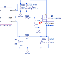
Part Number: UCC28730-Q1

Tool/software:

I have designed a 23 W Flyback-Converter with 1Outputs with a Inputvoltage of 250-800V and an Outputvoltage of 11V/2.1A.
I am now trying to put the PCB in operation, but I am facing unstable switching behaviours. The controller keeps restarting。I think the shutdown was caused by a reported fault。

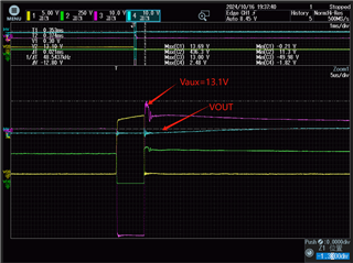
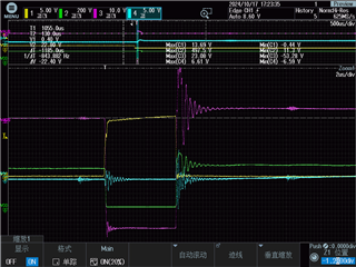
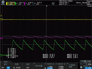
There is only one restart pulse(4.14us) as the green line(CH1:Vds  CH2:Vdd CH3:Vout)。

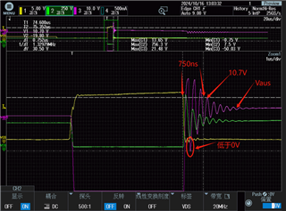
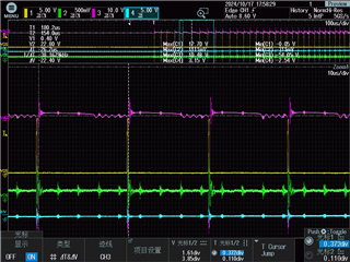
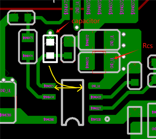
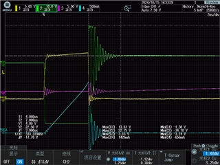
maybe the OVP or oc or uvlo fault.The actual test current did not reach the overcurrent point, and a 120pf capacitor was also added to the CS pin, which seems to have little effect(CH1:Vgs  CH2:Vaux CH3:Vout   CH4:Ids)。

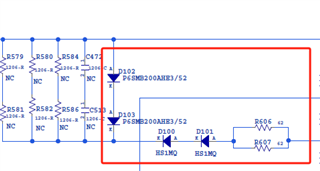
 the voltage of Vaux exceed 22.5V ,after the tlk-reset time, The voltage of Vaux does not exceed the overvoltage point(21.5V  RS1=121k RS2=33k),so

I don't think it's an overvoltage fault。I noted that the Vaux ringing Below Ground Can Trip UVLO,

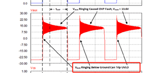
The actual voltage oscillation will also be lower than 0,Do you think UVLO triggered the system shutdown and how to solve it?What fault can cause a restart with only one pulse?

  • Hi Runbo,

    Thank you for reaching out.

    The cause for shutdown most likely from the AUX winding looks like OVP related shutdown. There is too much leakage ringing and this needs to be addressed with proper snubber design. This includes both primary and secondary snubber.

    Also ensure that the CS pin cap is placed very close to the pin and GND.

    Regards,

    Harish

  • Hello,Harish,

    Thank you for your response。

    I want to know how long the blanking time is? Look at this picture(CH1:Vgs CH2:Vds CH3:Vaux),there is too much leakage ringing on Vaux,but according to the data manual,the voltage on Vaux is not exceed 21.5V after Tlk_reset.I would like to know the basis for your judgment of overvoltage。Maybe my investigation direction is wrong,thanks!

    I also added some diodes to absorb spikes without  capacitors or resistors,but It doesn't seem to have much effect today。

     Rcs=0.82Ω,Transformer parameters Lp=1mH ,Np:Naux:Ns=120:17:11.

  • Hi Runbo,

    The blanking / reset time changes with load from 750ns at no load to 1.3us at full load.

    I would suggest using a RCD snubber with fast diode to help with damping the oscillations quickly

    Also consider placing the capacitor between pin 4 & 5 on top of the IC itself.

    Regards,

    Harish

  • Hello,Harish,

    Thank you for your response。

    I also added some diodes to absorb spikes with capacitors(4.7nF)and resistors(200k),The oscillation has weakened as shown(CH1:Vgs CH2:Vds CH3:Vaux CH4:Vout),but Vout looks abnormal with 1.7kΩ load),the IC still restarts。

  • Hi Runbo,

    Thank you for the reply.

    It looks like there could be 2 possible reasons.

    1. Ensure that the diode used in snubber is a fast diode with < 100ns recovery to see if this helps.

    2. Light loads generally arise if there is some noise associated with the Vs pin. Can you confirm the behaviour at higher loads and this only happens at lighter loads?

    3. I would recommend running the converter at stable load point and then slowly decreasing the load to the point where this restart occurs. At that point  I would recommend checking the frequency of operation of the converter just before restart. It will give a better idea on instability or potential noise affecting operation on Vs pin at lighter lods.

    Regards,

    Harish  

  • Hello,Harish,

    Thank you for your response。

    1. Ensure that the diode used in snubber is a fast diode with < 100ns recovery to see if this helps.

     ANS:yes,it is a diode with 75ns_max recovery time.I am trying to change the parameters of the RCD circuit with R=400K C=1.1nF,it doesn't have much effect either(CH1:Vgs  CH2:VDS  CH3:Vaux CH4:Vout)。

    2. Light loads generally arise if there is some noise associated with the Vs pin. Can you confirm the behaviour at higher loads and this only happens at lighter loads?

    ANS: with 100Ω-1k-10k-100k load,The phenomena are all the same under 350Vdc。

    Can you help me check if there are any issues with the schematic diagram and transformer design?Trandformer parameter: LP=1mH  NP:NA:NS=120:17:11800V backup supply--TI-UCC28730---20240925.pdfSLUC579_UCC28730 Design Calculator-20240913--case1.xlsx

  • Hello,Harish,

    I just tested the CS pin  voltage with a differential probe and found a different phenomenon,

    the IC applied many pulses and then the mosfet failed with G/D/S shorted as the photo shown(CH1:Vgs  CH2:VCS  CH3:Vaux CH4:Vout)。

    I'm not sure if the previous phenomenon is related to the CS pin?

  • Hi Runbo,

    That is an interesting observation.

    I think using this probe is probably causing the parasitic capacitance which the IC pin sees to be affected and probably affecting the timing causing IC to apply many pulses.

    Try putting the CS pin capacitor across pins 4 and 5 of the IC. Also it is better to use non isolated probe with low cap (<8pf) for probing the CS pin.

    Please let us know your observations.

    Regards,

    Harish

  • Hello,Harish,

    Thank you for your response。

    I may have found the reason。I cut the line on PCB of the mosfet of drive source pin and Vout turns normal with 10kΩ load under 350VDC。I think the current flows through mosfet to GND_UL  not through the sampling resistor,so the IC detected  the CS-pin fault。We will continue to test the circuit。This issue can be closed。Thank you for your prompt response。

  • Hi Runbo,

    Thank you for the feedback and good to know you were able to resolve the issue. 

    Regards,

    Harish