This thread has been locked.

If you have a related question, please click the "Ask a related question" button in the top right corner. The newly created question will be automatically linked to this question.

LM5156: driving an LDO (continued)

Part Number: LM5156
Other Parts Discussed in Thread: LM5157,

Tool/software:

I am resurrecting an old thread after getting distracted by other work!

https://e2e.ti.com/support/power-management-group/power-management/f/power-management-forum/1392212/lm5156-lm5156

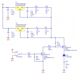
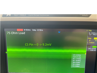
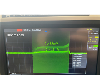
In this plot Vin is blue, Vout is yellow, and Switch Node is pin/purple. We switched to using a pulsed signal rather than a full on/off. I realize now you also asked for the CS pin, I will try to attack that addition later today.

  • same source signal, with the CS pin voltage added.

  • Hi Marsh,

    Can you please share your schematic?

    What are the exact specs of LM5157? Vin 12-32V? Vout 44V? Ioutmax=?

    The yello waveform in the first picture is Vout of LM5157? or Vout of your LDOs? Because its around 12V only.

    The CS waveform is not useful, please use a short GND wire for the probe or a barrel tip. Also the resolution should be like 20mV/ div.

    Best regards

    Moritz

  • Here is our schematic for the LM boost circuit:

    We have had 3 slight deviations from this, all discussed in the related but closed thread(s):
    - addition of an indicator LED
    - TVS diode at input
    - increasing output capacitance to 100uF per TI staff recommendation

    The target Vin is 24-28V. Vout 44V and Iout 6A.


    This board is driving a second board:

    I am having issues with the forum today so I am going to submit this while it is working. I will confirming the exact source of the Vout with my coworker and work on a cleaner CS signal and respond as I can. It might take until Monday for the CS signal, please do not close the thread.


  • for this image, i clarified that the yellow is the voltage across the load and the green is the CS pin voltage. even after using shorter leads the signal is still quite noisy, sorry about that. hopefully the delta is still enough to be of use for you. 

  • Hi Marsh,

    Just to clarify, because i am really not sure what i should help with right now:

    - You have problem with delivering the full output power, right?

    - Does the device even start up? Do you reach 44V aut the output without load connected?

    - What is the input voltage you are using in the scopeshot above? 12V ?

    - Why do you pulse this in 100ms cycles? Try do do a normal startup without pulses.

    - What means voltage across the load? I would like to see the Vout at the 44V rail.

    - The CS signal from above is not useful.

    Also the resolution should be like 20mV/ div.

    Also the time scale should be much lower. The reason why i want to see the CS signal is, that i want to check if you are hitting current limit. I have to see the signal in a resolution where i can see cycle by cycle.

    Please provide the following:

    scopeshot with Vin, Vout (44V), Swittchnode and CS at startup (can be zoomed out, just want to see if the device is switching and reaching the output voltage.)

    Then please a zoomed in version, where i can see CS.

    Best regards

    Moritz

  • Hello1 First off, thanks for taking the time to help.

    To take a half step back, we are working with a circuit and boards designed by a colleague who departed before being able to test and verify his design. At the surface, none of it seemed unmanageable and the designs seemed to be clear copies of WEBENCH recommendations and/or datasheet specified standard uses. 

    The circuit is in two stages on two boards. The first being the boost circuitry, which your colleague assisted us with here: https://e2e.ti.com/support/power-management-group/power-management/f/power-management-forum/1357874/lm5156-power-output-issues-at-full-load. After increasing the recommended capacitance we had success with the board while using a representative resistor load 

    The second stage is to take the output from that first stage and to use it to drive two parallel LDO’s setup as current sources. We have successfully operated this stage with a bench power supply. Our issues arose when using the boost circuit to power the second stage. 

    At this point, I am planning to start fresh with clean boards and step through things again, just in case we have damaged our test boards. With that in mind, I will try to get to some of your questions:

    You have problem with delivering the full output power, right?

    Correct. We were not getting the full 44V expected at the boost output and were getting roughly half the expected current when measuring across R26 in the above schematic. 

    Why do you pulse this in 100ms cycles? Try do do a normal startup without pulses.

    For all our initial testing of the boost circuitry we ran it ‘normally’ - a simple on/off operation with no pulses. We started using a pulsed setup for further testing as A. it is closer to what our end use will be and B. it seemed a little safer for our bench top testing. I am happy to revert back to simpler on/off testing if that would help. 

    Other questions are probably best answered after I get started with a clean board. I will try to respond with updates and scope shots by Monday, though it is possible that slips a couple days. Please don't close out the topic!

  • We are still working on this! Considering a re-spin of the board to better enable debugging. Will update as we can, please don't close this out yet. 

  • Hi Marsh,

    We will not close it.

    However, after 2 weeks of no acticity it will close itself.

    Best regards

    Moritz

  • Ok cool. Thanks Moritz. 

  • Sorry for the delay! I have been working with another engineer on this and we were struggling to get the stage with the LM5156 working, nevermind the LDO stage. Attached is the behavior with a 75ohm load across the ~44V output of the boost stage board with the design referenced earlier in this thread and the reference thread.


  • Below is the same operation with a 10 ohm load across the ~44V output. 

    We had previously had success with this same 10ohm load, incorporating the 100uF at the output stage that your colleague had recommended. In this case, we started with a fresh board and then changed the output capacitance. Nothing else has changed that we are aware of. 

    Any insight would be appreciated!

  • Hi marsh,

    Can you please reattach all relevant files?It is not easy to search through all the threads and posts over the time.

    The schematic would be important.

    In the first scopeshot all seems to be good, right?

    The current sense signal should be measured zoomed in do that single cycles are visible. Here, i can only see noise. Also it is important to use a very short ground connection.

    In the second scopeshot it is starting up but then shuts down. What happens later? Does it try to start up again?

    For the CS signal, please refer to above.

    Best regards

    Moritz


  • This is the design we used, with the only differences being a TVS diode at the input and 2 indicator LED's. Your colleague had no concerns about any of them. 

    Yes, the first scopeshot all is well. It is the 2nd set, with the larger load, where there is an issue. We have plans to come back to this later today, so I will hopefully have a better CS shot by then.

  • Hi Marsh,

    I am looking forward for the scopeshots.

    Best regards

    Moritz

  • Apologies for the delays, we are coming back to this issue as time allows.

    In trying to debug the issue as well as get you better images to work with we have done a bit of retooling of our test setup. Naturally, in our most recent effort, it seems the board was again working as intended. Not sure what changed in the meantime, so I am for now assuming we had a poor connection to the power supply at some point. 

    That said, I would love for a sanity check that things are looking as they should be for we reintegrate the LDO stage of our circuit. This scopeshot shows the Vout in yellow, sitting nicely at ~44v. The purple signal is the CS node - we were pleased to see a neater signal and are hoping that this is the expected behavior. 

    If this looks as it should then we will carefully reintegrate the LDO portion of the circuit. The boost circuit shown above has never succeeded in delivering the power to the LDO portion of the circuit, so we expect that behavior to continue. Assuming it does, I will try to get Vin, Vout, Switch node, and CS from the boost circuit again as well as include a schematic of the LDO stage.

    Thanks!

  • Hi Marsh,

    Thanks for using e2e. Due to the Christmas holidays, most of our team is out of office, and will return on the 7th of January. Please expect some delays in our response. Thanks for your understanding.

    Kind regards,

    Federico

  • understood! will reconvene then.

  • Hi Marsh,

    Our engineer is out of office, and will return on the 7th of January. Please expect some delays in our response. 

    Best Regards,

    Feng

  • Hi Marsh,

    The shape of the CS signal seems normal, hohever, there is a lot of noise on it. Is this noise really there or is it coming from your measurement setup? Are you measuring with a very short ground connection?

    Before adding yor LDO circuit again, did you already check with a resistive load? And see how much power can be drawn? I think this would be a good start.

    Then also please include all relevant waveforms.

    Best regards

    Moritz