This thread has been locked.

If you have a related question, please click the "Ask a related question" button in the top right corner. The newly created question will be automatically linked to this question.

LMG1210: About Schematic

Part Number: LMG1210

Tool/software:

Hi all,

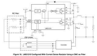
1) Referring to Figure 18 in the datasheet, I am considering changing the GND of LMG1210 to the source of the Lowside FET.
I think I can avoid potential fluctuation of the GND due to sense resistance.
In EVM, current detection is done at the end of the inductor, so I think it is possible.
Can I have the Gerber data of EVM and the pattern circuit diagram for reference?

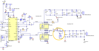
2) In the circuit diagram of EVM, R3 and R10 are designed to be 0Ω, but is it correct to use the gate resistor?

Best Regards,

Ryusuke

  • Hello Ryusuke,

    1) The Gerber and altium files can be found on the LMG1210EVM page.

    2) R3 and R10 are 0 Ohms for the fastest switching speed but if there is too much ringing on the driver outputs, the gate resistance can be increased to damp the ringing.

    Thank you,

    Walter

  • Hi Walter,

    2) R3 and R10 are 0 Ohms for the fastest switching speed but if there is too much ringing on the driver outputs, the gate resistance can be increased to damp the ringing.

    →Could you please confirm in detail what and how the constants of R3 and R10 change?
    With the time constant of gate resistance and gate capacitance, the change of gate voltage becomes gradual.
    As a result, the switch time between source and drain is extended, and ringing is reduced?
    At that time, since the switch time is extended, the power consumption inside the FET increases, and the efficiency decreases?

  • Hello,

    Please refer to this application note on how to choose a gate resistor and its effects.

    https://www.ti.com/lit/ab/slla385a/slla385a.pdf

    Thank you,

    Walter