
- Ask a related questionWhat is a related question?A related question is a question created from another question. When the related question is created, it will be automatically linked to the original question.
Tool/software:
Dear TI support,
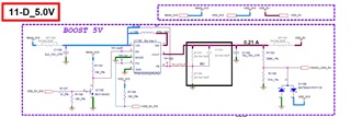
We are using TPS610333QDRLRQ1 as BOOST from 3V3 to 5V with current output load up to 0.21A
Here below the detailed schematic
We observe 2 behavior which are not expected according to the configuration mode chosen
1-Output voltage ripple of around 170mW and our target is below 100mV

2- Big overshoot and undershoot in the switching frequency captured at inductor testpoint

Could you please check the schematic and setting value and provide us with the good configuration and corrective values for the following objectives :
- Reduce the output voltage ripple below 100mV
- Eliminate Undershoot and overshoot in the switching frequency (inductor)?
Thank you for you quick feedback
Best regards,
Karim


