This thread has been locked.

If you have a related question, please click the "Ask a related question" button in the top right corner. The newly created question will be automatically linked to this question.

UCC28711: UCC28711:

Part Number: UCC28711

Tool/software:

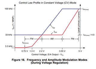
This is an excerpt from the UCC28711 datasheet.

The image implies that once the average output current reaches the regulation reference, the controller transitions to frequency modulation mode to regulate the output. It also states that the voltage is maintained below the regulation target and VDD is kept stable.

Please confirm if my understanding is correct:

  1. The VCST (Maximum CS threshold voltage) of UCC28711 is 780mV when Vvs is 3.7, and 195mV when Vvs is 4.35.
  2. The Vvs regulation reference (Vvsr) is 4.05, and the controller strives to maintain this value.
  3. When a load is applied to the output, as described earlier, the regulation reference in the average control block is reached, and the system transitions to frequency modulation control.
  4. At this point, the VCST level is increasing up to 780mV according to VCST(max).
  5. After, the VCST value is measured at approximately 780mV regardless of the load magnitude.
  6. However, if the Vvs voltage exceeds 4.05, the duty cycle will be adjusted, leading to a lower observed voltage. This is because the system has already entered the frequency modulation control region, and the frequency is adjusted to regulate the duty cycle.

Is my understanding correct?


The reason I am asking this question is that in an SMPS rated at 24V/2A, I observe that the VCST value measured at the CS pin remains approximately 700mV, regardless of whether the load is 0.3A or 1.5A.

This behavior seems consistent with the datasheet's description of the controller's operation in frequency modulation mode and the relationship between VCST and Vvs. However, I would like to confirm if this is expected behavior based on the design and regulation mechanism of UCC28711.

  • Hello,

    Please see my comments below.

    1. The VCST (Maximum CS threshold voltage) of UCC28711 is 780mV when Vvs is 3.7, and 195mV when Vvs is 4.35.
      1. If the output voltage is in regulation VS at the sample point should be 4.05 V (VVSR). 
    2. The Vvs regulation reference (Vvsr) is 4.05, and the controller strives to maintain this value.
      1. Vvs at the sample point will be 4.05 V when the output voltage is in regulation.
      2. When the output is in regulation and goes from full load to no load the peak current and frequency will be adjusted to maintain the ouput voltage based on control law shown below.  
      3. If the output is low and the desing is oppearating at constant current the design will be opperating at the maximum switching frequency.  Vvs at the sample point will be based on (Vout+Vdiode)*Na/Ns.
    3. When a load is applied to the output, as described earlier, the regulation reference in the average control block is reached, and the system transitions to frequency modulation control.
      1. When the output is in regulation and the load decreases the design will opperated based on control law.  Figure 15 from the data sheet shows how the freqeuncy and peak current vary with load.
    4. At this point, the VCST level is increasing up to 780mV according to VCST(max).
      1. VCST will be controlled 780 mV when the converter is opperating in the upper FM band.  E/A output is between 3.55 V and 5 V internaly to the IC.  The E/A output cannot be measured externaly.
    5. After, the VCST value is measured at approximately 780mV regardless of the load magnitude.
      1. This is not true.
      2. If you designed for the maximum frequency 100 kHz at maximum load the peak current will be controlled to VCST(max) of 780 mV down to roughly Pmax*100*44kHz/133kHz = 33% load.
      3. When the load decreasses below 33% you will enter the AM band when EA output is between 2.2 and 3.55V.  In this area of opperation the converter opparated at a fixed frequency of 44 kHz and modulate the peak current based on VCST(max) to VCST(min) of 195 mV
      4. As the load drops the E/A output will drop below 2.2 V.  When E/A output is below 2.2 V VCS will be controlled to 195 mV peak/
    6. However, if the Vvs voltage exceeds 4.05, the duty cycle will be adjusted, leading to a lower observed voltage. This is because the system has already entered the frequency modulation control region, and the frequency is adjusted to regulate the duty cycle.
      1. When the output is regulation if the output tries to go over regulation EA OUTPUT will decrease and adjust the peak current and frequncy to maintain the output.  Please refer to the above control law.

    Regards,

  • Thank you very much for your thoughtful response. It helped me understand many of the confusing points. However, I still have a few questions:

    1. In your response, I am curious about the parameters used in the equation. I understand that 33kHz corresponds to the frequency in the AM region. What does 44kHz represent?

    2. I measured the CS pin and GND pin of the PWM IC using an oscilloscope with a passive probe, and I observed a value of about 1V in some cases. I assume this measurement might be incorrect due to noise components caused by parasitic inductance. Would this assumption be reasonable? The SMPS is operating stably.

  • Hello,

    1.  I made a typo it should have been 33 kHz and not 44 kHz.  Sorry about that.

    2.  If you power supply is stable the measurement may not be correct.  You might want to recheck that just to make sure it is correct.

    Regards,