This thread has been locked.

If you have a related question, please click the "Ask a related question" button in the top right corner. The newly created question will be automatically linked to this question.

UCC21521: dual gate driver SiC slow switching

Part Number: UCC21521

Tool/software:

Dear TI design support,

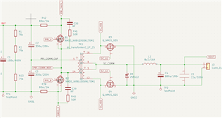
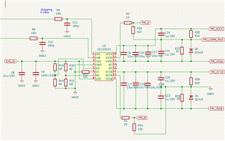
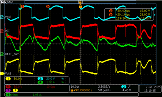
I experience the slow intermittent switching in half-bridge and dual gate driver UCC21521, I used negative stage bias with Zener diods for my SiC MOSFETs and wonder why the gate signals are so noisy and especially VdsB (bottom MOSFET) with slow rising edge. I added multiple MLCC caps on VDDA, VDDB side of the driver, very near to the driver and still see VDDA, VDDB fluctuates and the switching is poor.

  • Hi Darek,

    This looks to be a repeat of your previous post. Please focus on one thread. Hiroki gave good advice about maybe increasing R36 and R38 to only what is required for Vz, and reduce the DC current load on your isolated power supplies. With 820 ohms it will be over 20mA of load current. You probably only need 1mA.

    It looks like your power rails have a low frequency oscillation, based on the blue VgsB line here. Can you share the schematic of your PRI_VCCA and PRI_VCCB supplies? The gate driver will only be as strong as its power supply, since it is at best a closed switch to the power rail.

    Best regards,

    Sean

  • Hi Sean,

    Yes right, I am trying from a different angle to find some answers to the more thorough problem I posted in another thread. Here I just show the case when power supply works in CCM mode but anyway at switching moments Vds is very poor, it changes fast in the first phase but then it rises then falls again.

    PRI_VCCA and PRI_VCCB are from PCB connector, they come from two independent channels of an external power supply set 22V, they have to be independent as negative stage bias will not function well with bootstrap diode. I added Polymer Cap + MLCC Cap (220uF + 22uF) near those connectors but anyway the voltages fluctuates 18 - 26V, they may have resonance character, as it looks like sinus.

    Your second thought about the Zener current... it can be stolen when driver sinks gate(MOSFET) current, then the offset will not be 4.3V but 2V. What should be the right balance of those currents? Zener current 1mA is not too low? Driver is capable to sink even couple of Amps. Maybe I should get rid of R33, R34 to prevent that?

    Regards

    -Darek

  • Hi Darek,

    I think it will be best to continue this discussion in your other post. 

    You should first investigate the stability of this external supply. It seems that the inductance of the connection might be resonating with your local decoupling.

    How large is your gate charge? When the gate driver sinks current, the decoupling capacitors provide the instantaneous gate drive current, both positive and negative. It should not droop from 4.3 to 2V if it is 20x the size of the gate capacitance. The Zener diode should start to conduct more current when the voltage droops; it does not necessarily need to conduct high steady state current to maintain the charge on the decoupling capacitors.

    Best regards,

    Sean

  • Dear Sean,

    I just did a test with my PCB where this time I used 3 separate external volt sources: BATT, VCCA, VCCB and SYS_12V. VCCA, VCCB = 22V.

    The bad noise has gone. The MOSFETs work fine, no problem with switching loss, VgsB is very clean, VdsB as well, it has a bit of ringing at dead-time period but this is far better now.

    The external power supply has got 3 channels and though there is no dc connection between GND1 or GND2 or GND3 it seems there is a capacitance coupling and then it shorted my VSSA and VSSB.

    Many thanks for your suggestions. 


    Regards

    -Darek