This thread has been locked.
If you have a related question, please click the "Ask a related question" button in the top right corner. The newly created question will be automatically linked to this question.
Tool/software:
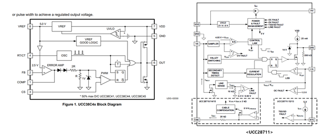
1.These are two PWM ICs from TI.
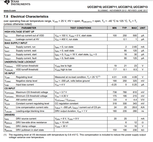
2.The 3844 series has output voltage and output current specified in the datasheet. The block diagram also indicates the output voltage. The output current is correlated with the current flowing through VDD.
3.In the case of the 28711, it functions as a current source. There is no mention of the output voltage in the datasheet. Therefore, the output voltage is related to the load connected to the PWM IC. This is also limited to 14V by a Zener diode.
Is my understanding correct?
Hello,
The 3844 is an older device that use N channel and P channel FET to drive the external FET. The upper FET is directly tied to VDD and requires an external resistor from output the devicde to the external FET's gate to limit the current. The UCC28711 is a zero current switched flyback controller and does not require as much drive current as the 3844. So the designer chose use a 25 mA current source to drive the FET.
In regards to the voltage at the drive pin of the UCC28711 it is tested with a VDD of 25 V and gives a measured drive clamp voltager of 14 to 16 V. This is the internal zener clamp diode measured at the DRV pin.
Since the DRV pin is driven with a current source this is high impeadenance. If VDD is below the clamp voltage, the DRV pin after charging the FET's gate capacitance should reach VDD.
Thank you for interest in Texas Instruments (TI) products. If you have a related question, please click the "Ask a related question" button in the top right corner. The newly created question will be automatically linked to this question.
Regards,