This thread has been locked.

If you have a related question, please click the "Ask a related question" button in the top right corner. The newly created question will be automatically linked to this question.

UCC21710-Q1: Simulation for UCC21710-Q1 using PSPICE for TI

Part Number: UCC21710-Q1
Other Parts Discussed in Thread: UCC21750

Tool/software:

Dear Sir,

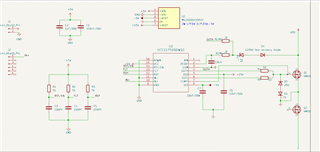
I am New to PSPICE for TI. I want to simulate and understand the functions of the IC. So please share any reference simulations available for 

UCC21710-Q1

Thank you.

  • Hi Sravan,

    We do have the PSPICE model in the following link,

     UCC21710 PSpice Transient Model

    There are no example simulation projects - however we have the following schematic example for our EVM, which can be used to generate a simple project for your evaluation.

    UCC21710QDWEVM-054 Schematic Files

    Hope it helps

    Thanks

    Sasi

  • Hi Sir,

    Good Morning. Have a nice day.

    Is there any dead time setting possible with this UCC21710-Q1  part gate driver?

    Thanks,

    Sravan kumar.

  • Hi,

    I have doubts in calculating the source current and gate resistor. The way i have followed:

    MOSFET used: FF2MR12KM1H  has Qg=1.2uC and Traise = 153ns (from the test conditions given in datasheet of mosfet).

    Isource = Qg/tr = 1.2uC/153ns = 7.8 A so I choose 10A gate driver and for gate resistor = Vg/Isource = 18/7.8 = 2.3Ohms.

    Please, tell weather it is correct or suggest how to calculate the source,sink current and gate resistor.

    Thank you.

  • Hi Sravan,

    No the device doesnt apply any dead time how ever, OUT will be high only when INP=H and INN=L. Hope it helps.

    Peak current based on all the resistances in the gate loop path can be computed as shown in the formulae below.

    SLUC695  UCC217xx XL Calculator Tool

    The switching frequency and gate capacitance defines the driver thermal behavior. So the system needs to be defined based on all the considerations.

    Hope it helps.

    Thanks

    Sasi

  • Hi Sasi,

    I have designed a Gate driver using UCC21750.Here I am attaching the design. Please review and tell is it ok or not if any suggestions please let me know.

    I have following doubts with the design please clairfy:

    1. I came to know about the 2 decoupling capacitors 1 for the high frequency noise rejection with low capacitance and for good voltage stability high capacitance is needed. With single capacitor it may not possible to have above two functions. I know abt the thumb rule like for small caps 100nF-1nF and for large caps >1uF.  I want to know How to calculate of these Decoupling capacitors?

    2. is it necessary to keep a Input and output RC filter and reason? How to calculate the RC values for filter for operating frequency of 20KHz in detail?

    3.How to calculate the Pull up resistors? here I have used pull up resistors for RDY, FLT, REST pins as per specified values in datasheet 5Kohm and a filter capacitor of 100PF. How to calculate the Pullup resistor and filter capacitor 100pF?

    4. Regarding DESAT I came to know that DESAT threshold can be set by using Zener diode. I dont understand this one exactly how it works. Please Explain?

    5. Please explain How to calculate the DESAT circuit components Cblnk, Rlim.

    If possible can i connect through mail for better understanding of concept.

    Thanks for your time.

    Sravan Kumar

  • Hi Sravan, 

    Sasi is out of office and I can help with these questions. 

    For simulation, I suggest: 

    • Tying AIN to COM and leaving APWM floating if not used
    • Use the calculator tool Sasi provided to calculate the DESAT detection threshold. Looks like you have a 7V zener in the path, maybe that will make the DESAT detection threshold too low
    • In actual design, VDD-COM capacitors are needed to keep VDD stable

    To answer your questions: 

    1. Yes, we usually suggest one capacitor in the order of ~100nF and another in the uF range. System noise can range from a few MHz to hundreds of MHz, and having small decoupling cap, together with the parasitic resistance on the board, can help us filter out the system noise well. 

    2. I would recommend input RC filters, resistance ~100Ohm and capacitance in the tens of pF range. Again to filter out system noise. 

    3. 5kOhm - 10kOhm pull up resistors are sufficient. The RDY and nFLT pins are open drain outputs, and this resistor helps limit the current into nFLT/RDY when it's pulled low. 

    4. You can refer to this E2E: https://e2e.ti.com/support/power-management-group/power-management/f/power-management-forum/1011100/faq-ucc21750-how-can-we-adjust-the-desat-detection-threshold-in-ucc217xx-iso5x5x

    5. Recommend Rlim in the 1kOhm-10kOhm range. You can choose a Cblk value that best matches the DESAT timing you need. It's usually in the tens of pF to hundreds of pF range, please refer to the calculator tool Sasi provided. 

    Thanks,. 

    Vivian

  • Hi,

    Thanks for your reply. I want to know How to calculate Pull up/down resistor values, decoupling capacitor and RC filter values with suitable equations.

    2. The above attached design is ok for Hardware if not please rectify errors. is it possible to do simulation for this design!

    Thank you,

    Sravan Kumar.

  • Hi Sravan, 

    Cutoff frequency for noise is just 1/(2*pi*R*C). If you have a system noise frequency in mind you can use this equation. 

    Pull-up resistors are used to limit current into the pins. Current into the pins can be calculated by VCC/R where R is the resistor size. 

    You can try using PSpice for TI to run the sims. 

    Thanks, 

    Vivian