UCC28056: Switching waveforms look poor at 277VAC

Part Number: UCC28056
Other Parts Discussed in Thread: UCC256404

Tool/software:

I'm currently designing a 100W, 24V power supply and using the UCC28056 as a PFC-Boost controller to take a 120-277VAC input and put out a 450V DC Bus, which then goes through a DC/DC stage with a UCC256404 controller.

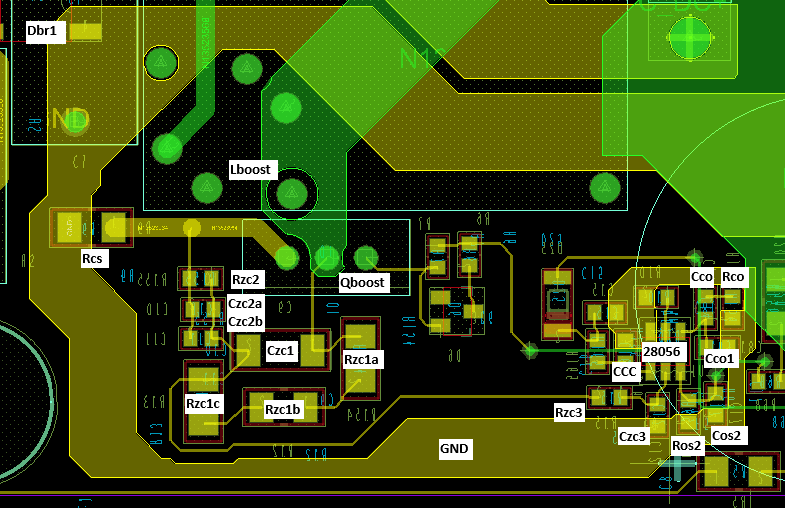
At 120VAC in, everything works great, but as I increase the input voltage, the switching waveforms of the Boost FET becomes a bit erratic, leading to poor input current waveforms and high power dissipation.  Attached are my schematic and excel design file, as well as scope plots.

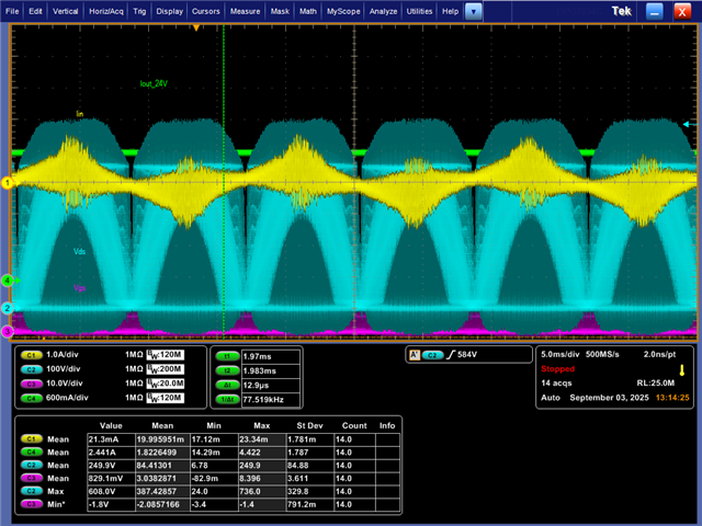
It looks like, at 277VAC, the voltage at the drain never rings close to 0V, like it does at 120VAC.  Is that expected?  The duty cycle and/or Fsw also seem to vary quite a bit at 277VAC.  Probing across the current sense resistor doesn't show anything odd.  I've tried probing the ZCD pin, too, but the converter doesn't like that and will declare a fault, so I can't get a good waveform for that.

Any help would be appreciated.  Thanks.

Boost PFC Sept3 20025.pdfUCC28056X_Design Calculator Aug18 2025.xls

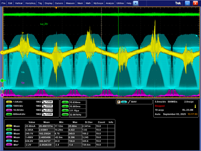
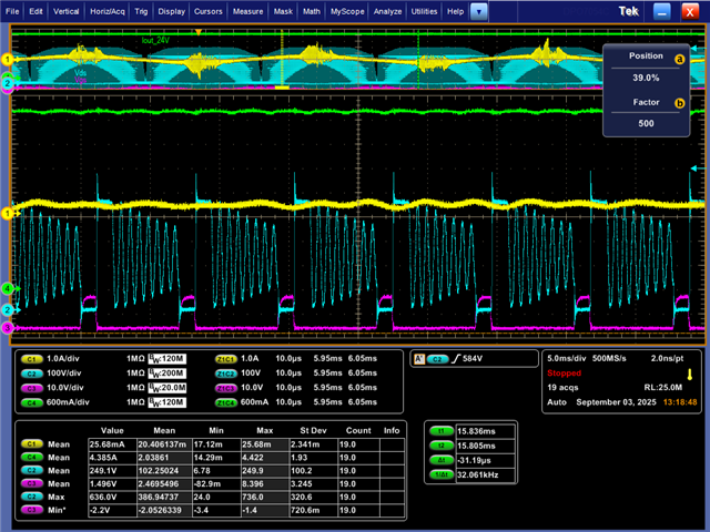
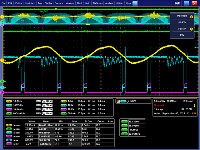
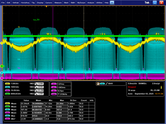
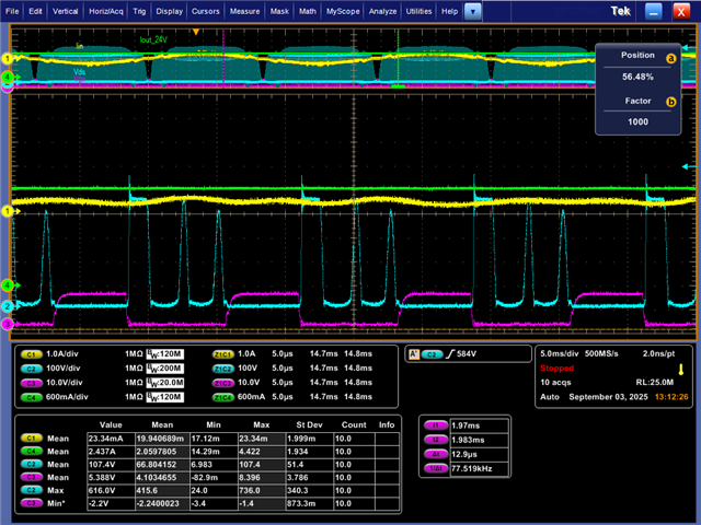
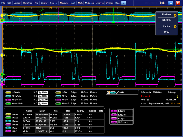
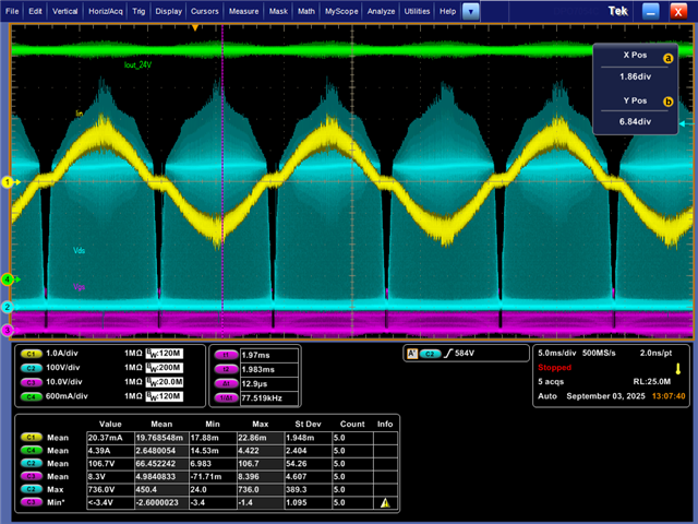
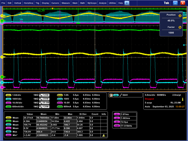
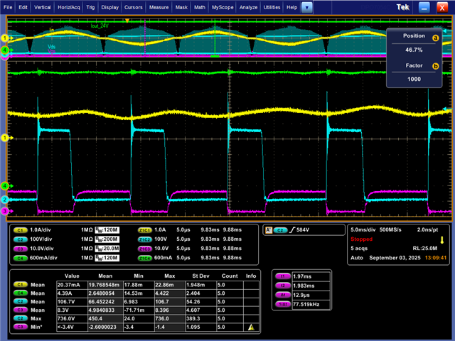
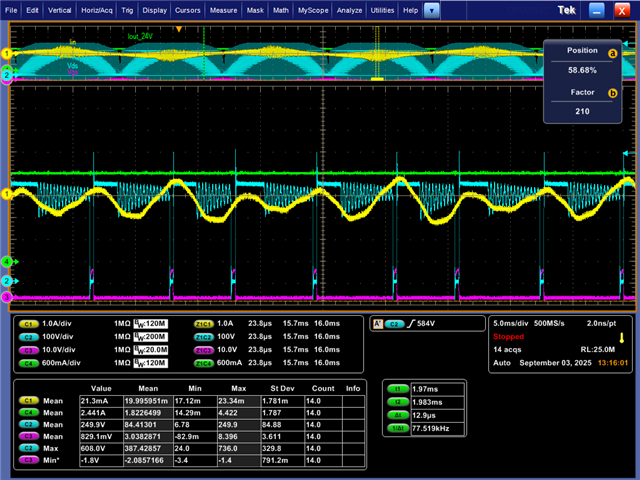
In the plots below, the green trace is the output current of my 24V rail (mostly irrelevant for this issue - it's just there as an indicator of how much power I'm pulling), the yellow is the input current from the AC line, the cyan is the drain-source voltage of the Boost FET, and the purple is the gate of the boost FET.

120VAC and 50W of output:

120VAC and 100W of output:

277VAC and 50W of output:

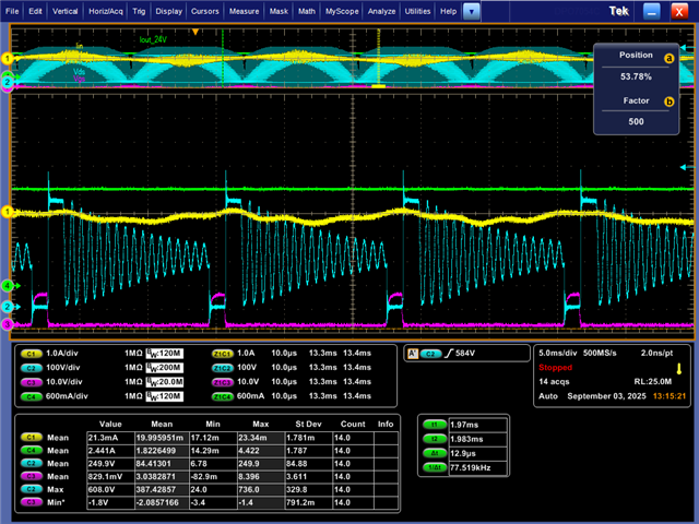
277VAC and 100W of output

  • Hi Joe,

    It seems that the PFC is going into DCM mode at high line input voltage. The same can also be seen in the waveforms of 120VAC/50W. During DCM operation, the average value of drain-source voltage during the DCM ringing is equal to the instantaneous input voltage. As the input voltage goes high, the average value increases, causing the drain-source voltage to not cross zero. That is an expected phenomenon. You can try the UCC28056 simplis model with the parameters of your application for better understanding: https://www.ti.com/lit/zip/slum620

    Regarding the poor input current waveform, it seems this is also due to the DCM mode of operation only. Please try increasing the current sense resistor to avoid the situation.

    Regards,
    Soumya

  • Soumya,

    Thanks.  I've tried getting this to work in Simplis, but I get a 'can't decrpyt the data' error when I try and simulate it.  I do only have the free version of simplis, if that matters.  I also don't use simplis very much, so I'm unfamiliar with a lot of how to get things to run.  The forum won't let me upload a .sxsch file.

    I'm just a little surprised that I'm still in DCM mode at full power (even at 277VAC).  My Rcs is about as high as the design file wants me to take it.  It's at 0.075 ohm, now, and if I try and increase that to 0.08, the excel file tells me to reduce the value.  I was also under the impression that the chip has ways of preventing itself from switching between DCM and CrM mode multiple times within the same line cycle (last couple of lines of section 8.3.3 in the datasheet).  At 277VACin and 110W out, I look like I transition multiple times across the line cycle (though typically only around the peak of the line - that's where my input current becomes very noisy).


  • Hi Joe,

    Sorry for a bit late response. Can you please share the schematic of your board?

    Regards,

    Soumya

  • Soumya,

    No worries.  There is a pdf of my schematic shared in my first post, as well as the design excel file.

    Thanks,
    Joe

  • Hi Joe,

    I tried to reproduce the issue in the simplis model with the parameters according to your schematic. It seems like I got the issue, just for confirmation, can you please send the inductor current waveform in 2 different input voltages (120V and 277V) and same loading condition in the same time scale what you have sent in the original post?

    Regards,

    Soumya

  • Soumya,

    Thanks for the help.  I don't think I have an easy way to directly measure inductor current on my design.  There no good place a current probe will fit.  I could probably mod the board, but it'd be cumbersome to do so.  But, if that's necessary, I'll do that early next week.

    I did take measurements across the current sense resistor, if that helps.  It's a 0.075 ohm Rcs.  I put horizontal cursors at 75mV and 150mV to denote 1A and 2A, respectively, just for ease of viewing.

    Yellow - Iin Purple - Vcs.zip

    Thanks,
    Joe

  • Hi Joe,

    It seems the issue that I suspected earlier is not the correct one. It might be caused due to noise coupled in the ZCD pin which cannot be visible in simplis simulation. As per the layout example given in the datasheet, the ZCD pin loop needs to be kept small and the components need to be kept near to the controller. Can you please confirm if these conditions are maintained in the layout?

    Also, can you check by increasing the input voltage gradually from 120VAC to 277VAC if the noise is coming suddenly at certain input voltage value or it gradually increases along with the input voltage?

    Regards,

    Soumya

  • Soumya,

    I think I'm leaning in that direction, as well.  I can't actually probe the ZCD pin, so I can't see exactly what its waveform looks like.  When I put a probe to it, the converter shuts down.

    Here's a snip of my layout, with things labeled similar to how they are in figure 36 of the UCC28056's datasheet (the ref schematic) -

    I do have the ZCD circuitry closer to the FET than I do the IC.  I was trying to minimize the length of trace from the Rcs/Qsource net into the ZCD components, but maybe that isn't the best way to do that?  I was also trying to keep the controller a bit away from the switching node of the converter.  I do need to update the artwork on the board for a handful of other reasons, so I'll take a closer look at this area when I do that.

  • I guess I'll also ask, since you put my values into Simplis.  Are you getting waveforms you'd expect from a properly running converter in Simplis, based on the component values I have?  As far as I can tell, at least at 120VAC, my board seems to be working well.

  • Hi Joe,

    Keeping the controller a bit away from the switching node is a good idea as that area has high noise. But the ZCD network needs to be kept very near to the IC as shown in the Layout guideline section in the datasheet. The idea to keep Rcs near to the ZCD network is also very good, but the distance from IC to the network is to be minimized with higher priority. It would be best if there is a way to maintain both the conditions, if possible. But sometimes it is tough to achieve.

    Regarding the simplis model, initially there also I got some noise in the input current (not as bad as your waveform though), but I could minimize it by reducing the bandwidth of the input filter. That worked in simulation, but that solution will not help in your case as the layout related issue is tough to reproduce in simulation.

    Regards,

    Soumya