This thread has been locked.

If you have a related question, please click the "Ask a related question" button in the top right corner. The newly created question will be automatically linked to this question.

LM5118

Other Parts Discussed in Thread: LM5118

Hi,

I am trying to design a buck-boost  regulator around LM5118 and I want use the below parameters:

Vin= 23 to 34V DC.

Vout= 28V DC.

Iout= 5A.

When it doesn't any load the output voltage is 28V but when a load with 0.3A connected to output the voltage reduced to 16.6V.

I used IRF2807 (VDSS = 75V ,RDS(on) = 13mW, ID = 82A ) for Q1 and IRFZ46N (VDSS = 55V , RDS(on) = 16.5mΩ , ID = 53A ) for Q2 and MBR760 for diod.

Please help me.

  • Hi

    Please check your current limit. It is possible your current limit setting is too low since you have the issue with load while there is no issue without load.

    Regards,

  • Hi Eric,

    I don't understand where I Should check?

    I used from WEBENCH  and I set that parameter on my PCB.

    I set in WEBENCH 5A for Iout.

  • Hi

    Please check your Rsense value whether its too big or not. Or you can simply put one more Rsense on top of your current Rsense and then see whether there is an improvement or not.

    Regards,

  • Hi Eric,

    Rsense= 0.01R ,5W , Nickel-chromium like this picture

  • Hi

    This is too inductive. It will generate a lot of noise. Please use SMD type sense resistor. The distance from the source of power diode to PGND pin is recommnedned to be below 1cm.

    Regards,


  • Thank you very much.

    My problem was for this resistor? (I have doubt but I don't find SMD package for this value )

    If I change my resistor my problem will be solve?

  • Hi

    I cannot guarantee any, but I believe if you improve your design items one-by-one, your converter will work well eventually.

    Right now, it is for sure that such a cement resistor is not a good choice for the sense resistor.

    Regards,

  • Hi Eric,

    I found and ordered the SMD resistor for Rsense and replace to cement resistor but my problem is not solve yet.

    I installed two 0.018R parallel that equal 9 m ohm.  

    please help me.

  • Hi

    Would you share your layout, latest schematic and BOM ?

    Regards,


  • Hi,

    I am not in home and I share 2 pdf file.

    The first one is my schematic file that shared before but the value is not true. I changed the value according to second PDF file.

    1- 0363.8765.LM5118-Schematic.pdf

    2-5618.webench_design_3595001_19.pdf

  • Hi

    I need the layout and BOM.

    Regards,

  • Hi

    I shared the last schematic and PCB file in PDF.

    If it need I share Altium file.

  • Hi

    I shared the last schematic and PCB file in PDF.

    If it need I share Altium file.

    3568.LM5118.pdf

  • Hi Saeid


    I think it is extremely hard for power electronics beginners to make high speed switching regulator working properly with one layer board.
    It is better to re-layout your board based on the reference layout (Please refer http://www.ti.com/general/docs/lit/getliterature.tsp?literatureNumber=snva334&fileType=pdf) or order LM(2)5118 EVM at http://www.ti.com.
    When designing a high frequency switching regulated power supply, layout is very important. Using a good layout can solve many problems associated with these types of supplies. Please refer www.ti.com/lit/an/snva021b/snva021b.pdf


    Regards,

    Eric

  • Hi Eric,

    Thank you very much for your information.

    I study the second PDF file about layout that very useful for me, but I cannot download the first link.

    I decide to design a new board on 2 layer according to this information but before that I want to sure from some of my parts.

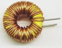
    The first one is Inductor that twist by myself like below picture but the diameter of wire is 2 millimeter without any cover.

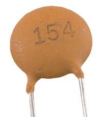
    The second part is ceramic capacitor for Ccomp=270pf like below picture

    Which of my diode should be near the PGND pin? please say the number of diode from my schematic.

    And finally please say every point that should be do.

    Thanks.

    Regards,

    Saeid

  • Hi Eric,

    I have a question about ground of circuit. In this IC we  have 2 ground, that I want trace one of them on the top layer and the other one trace the bottom layer and then connect them with a via. this work is true?

    I want install the inductor on top layer, which ground should be on top layer?


    Regards,

    Saeid

  • Hi

    Please connect both grounds on the same layer which LM5118 is mounted, beneath the IC.

    A ground plane in the PC board is recommended as a means to connect the input filter capacitors to the output filter capacitors and the PGND pins of the LM5118.
    Connect all of the low current ground connections (CSS, RT, CRAMP) directly to the regulator AGND pin. Connect the AGND and PGND pins together through topside copper area covering the entire underside of the device. Place several vias in this underside copper area to the ground plane of the input capacitors.

    Regards,


  • Thank you very much for response.

    I asked 2 question that one of them is on the first page which probably you not saw.

    On that PDF file wrote :

    It would also be a good idea to have a ground plane on both sides of the PCB. This will reduce noise as well by reducing

    ground loop errors as well as by absorbing more of the EMI radiated by the inductor

    Regards,

    Saeid

  • You eventually need ground on both ides because the DAP connection of LM5118. Please read through datahsheet and review the layouts in the Application Note http://www.ti.com/general/docs/lit/getliterature.tsp?literatureNumber=snva334&fileType=pdf


  • I am sorry Eric, I asked very question from you.

    Until now I design 3 boards and I  want this board will be the last one.

    This question is the last question for design part.

    Please say which parts should be near together?

    you forget answer this question in the first page

    Hi Eric,

    Thank you very much for your information.

    I study the second PDF file about layout that very useful for me, but I cannot download the first link.

    I decide to design a new board on 2 layer according to this information but before that I want to sure from some of my parts.

    The first one is Inductor that twist by myself like below picture but the diameter of wire is 2 millimeter without any cover.

    The second part is ceramic capacitor for Ccomp=270pf like below picture

    Which of my diode should be near the PGND pin? please say the number of diode from my schematic.

    And finally please say every point that should be do.

    Thanks.

    Regards,

    Saeid


    Thanks a lot.

    Regards,

    Saeid

  • These are combinations of components which should be placed close each other

    Cin-BuckMOSFET-Buck Diode

    Cout-Boost MOSFET-BOOST Diode

    ground connection of Cin - ground connection of Cout

    Cvin-Cvcc-Chb-LM5118

    AGND-PGND-DAP

    HO-HS-gate of buck MOSFET

    LO-PGND-gate of boost MOSFET

    Ccomp-Chf-Rcomp

    Rfb_top-Rfb_bot-AGND

  • Thank you very much.

    finally you did not answer the last question on the first page.

    I write it here  :

    Hi Eric,

    Thank you very much for your information.

    I study the second PDF file about layout that very useful for me, but I cannot download the first link.

    I decide to design a new board on 2 layer according to this information but before that I want to sure from some of my parts.

    The first one is Inductor that twist by myself like below picture but the diameter of wire is 2 millimeter without any cover.

    The second part is ceramic capacitor for Ccomp=270pf like below picture

    Which of my diode should be near the PGND pin? please say the number of diode from my schematic.

    And finally please say every point that should be do.

    Thanks.

    Regards,

    Saeid

  • Hi Eric,

    I changed the position of my parts according to datasheet,your suggest and layout guidelines for switching power supplies.

    Please check my layout specially inductor position,Diodes position and MOSFET position.

    What is Chf? you said Ccomp-Chf-Rcomp should be placed close each other.

    Please say your opinion about my inductor which it like above picture.

    Thanks.

    5584.LM5118.pdf

    Regards,

    Saeid

  • Hi Eric,

    I complete my layout that shared on previous post and share for you.

    Please check my layout and say the bugs.

    5280.LM5118-2.pdf

    Thanks a lot.

    Regards, 

    Saeid