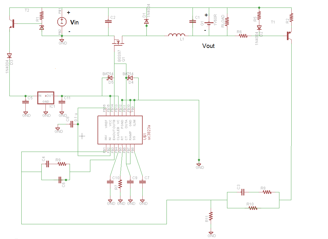
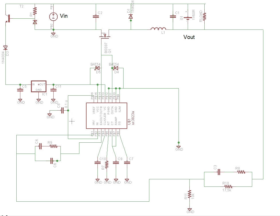
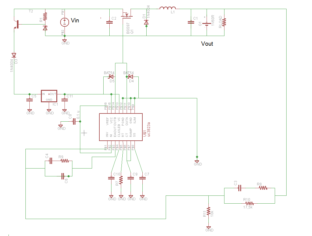
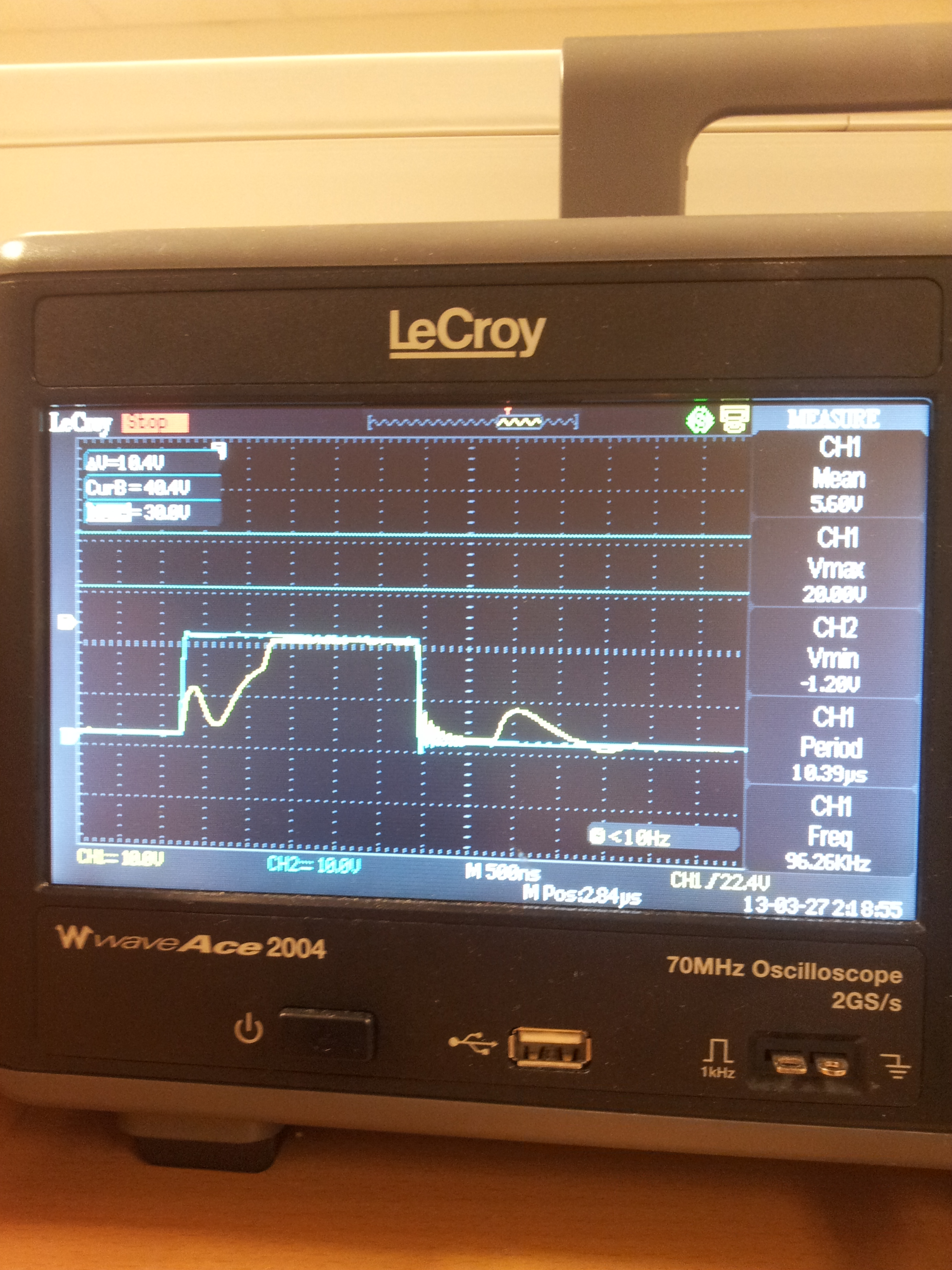
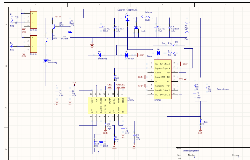
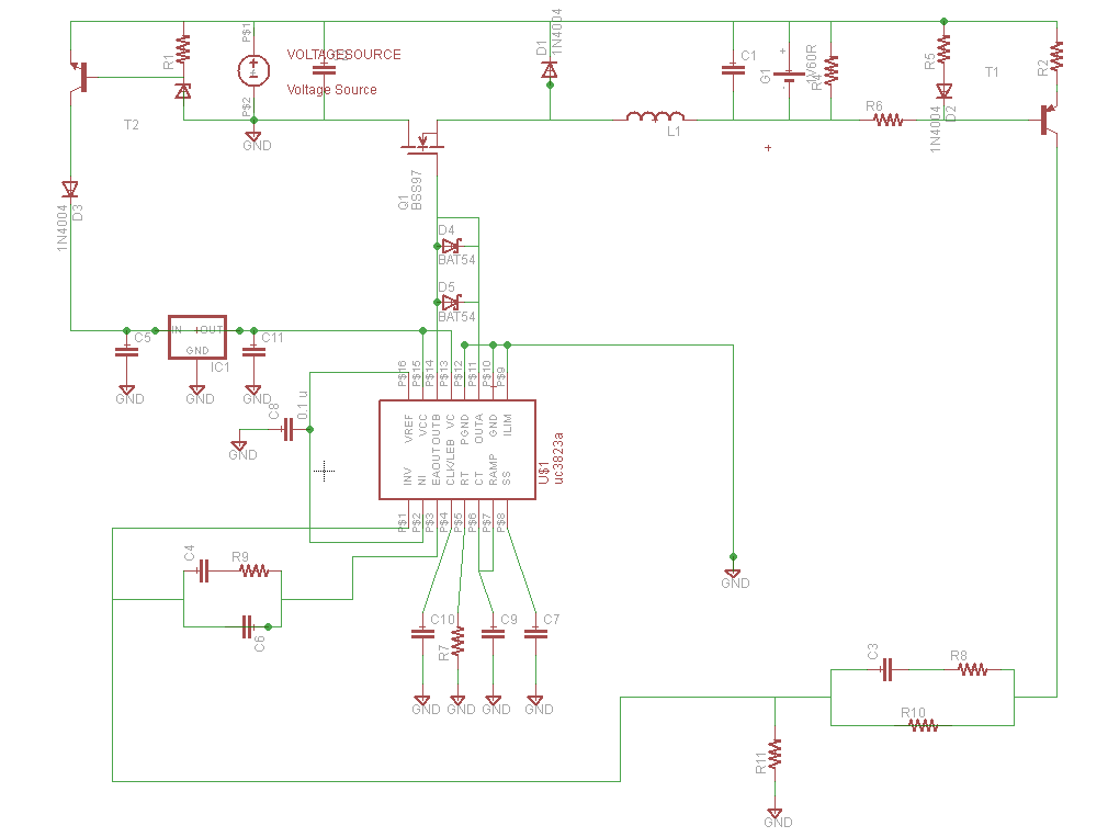
Hello. I'm building a buck dc/dc power supply with the UC3823a pwm controller. How do I control the Pwm signal? I don't understand how i should calculate the value of my resistors and capacitors. Can anyone help me understanding the pwm controller.

-
Ask a related question
What is a related question?A related question is a question created from another question. When the related question is created, it will be automatically linked to the original question.