


I was looking at the EVM design and noticed that on the output grounds and both voltage outputs there is a split in the copper pour going to the headers (J4-J7). I haven't seen that done before and wondered why the board was designed like this.
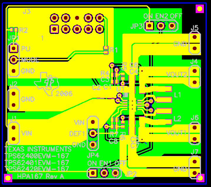
I was looking at the EVM design and noticed that on the output grounds and both voltage outputs there is a split in the copper pour going to the headers (J4-J7). I haven't seen that done before and wondered why the board was designed like this.

