This thread has been locked.

If you have a related question, please click the "Ask a related question" button in the top right corner. The newly created question will be automatically linked to this question.

LM5006 ringing

Other Parts Discussed in Thread: LM5006

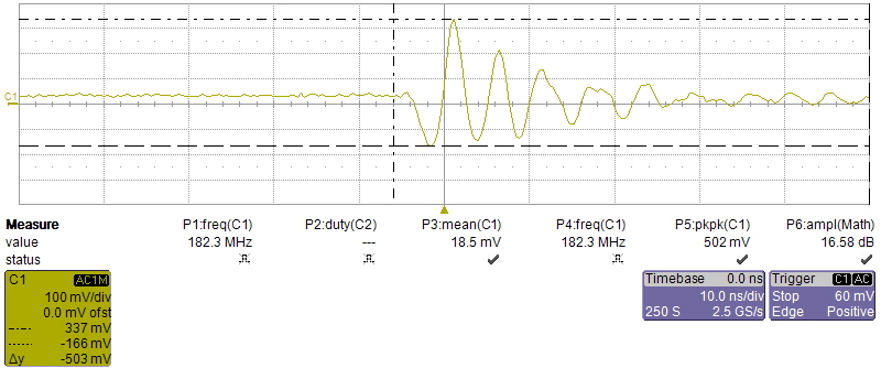
I'm currently using the LM5006 and recently took it in for EMI testing and found that there was a lot of noise around 185MHz.  Upon closer investigation, there is ringing at 185MHz at every switching cycle.  I see the ringing everywhere (Cin, Cout, etc) so I'm not sure exactly where it's coming from.  I have the LM5006 Eval board, and I see the same 185MHz ringing on that board, so it's not due to flaws in my layout (or at least not flaws that aren't shared by the eval board). 


Some component values:
Cin is 1uF, 0805 and 0.1uF, 0603.
Cout is 15uF, 1210
Inductor is 82uH. 
I am using a diode for the freewheel switch, PMEG6020ER,115

Outside of the ringing the circuit has performed very well (accurate, efficient, etc).  I have input and output wires which are probably responsible for the EMI and I'm prepared to use appropriate ferrites to keep the noise from radiating.  HOWEVER - it would be great to add an additional capacitor or two and reduce the noise at the source, rather than just relying on the ferrite.  Given that the ringing is reproduceable on the eval board, could you (or anyone) recommend any particular tweaks that could help?

A screenshot of the ringing at Cin (AC coupled)

  • It is common to see ringing and overshoot on the switching node due to fast switching currents and circuit parasitics. The usual method to control it is with an RC snubber from SW to GND.
  • Thanks John, I'll give that a shot.

    - Any particular recommendations for R and C, at least as a starting point?
    - Will this have any affect on the boost capacitor?
  • I usually use this approach:

    5047.RC Snubber.pdf

    It should not cause any issues with the Boost cap operation.

  • Thanks John.

    A question about the power dissipation of the snubber. In the example the snubber loses 32.8mW, and that loss appears to be constant and more or less independent of the load. Efficiency is critical in my system so I'm a little wary of that loss. On the other hand, a ferrite with a DCR of, say, 50mΩ at an input current of 500mA (the max I will see) will dissipate just 12.5mW, and that will go down with load.

    So - if efficiency is very important for me, and my concern is radiated EMI (rather than any affects of the ringing on the load, etc), might a ferrite make more sense for me? Or would you recommend focusing on eliminating the ringing at the source as a better solution?
  • Ferrite between the output of the converter and the load?  I typically am in favor of eliminating the noise rather than filtering it.  But you are correct, there is no free lunch,the snubber will cost in efficiency.  It is your call,

  • I am more likely radiating from my input wire so the ferrite will probably go between the input and the converter.  I'll add a pad for one on the output in case that is needed as well (my product is just the power source, so the load is connected by the user to the end of an output wire).

    A question about C5, the smaller input capacitor.  The datasheet says this is to avoid ringing at Vin - if my ringing is due to the SW node, I assume that no change to C5 will make much difference?

    And a (perhaps) naive question about the snubber - why is the resistor needed?  Why can't the capacitor simply act like an AC bypass and shunt the high-frequency to ground, without needing the resistor?

  • John - looking closer at my layout vs. the eval board, I notice that the eval board has a top-level ground plane for C3, C5, pin 4, and D1, but that the plane is only connected to the bottom plane through 3 vias around D1. My layout has a similar top-side plane, but there are stitching vias everywhere, including under the regulator and closer to C5 and C1.

    Would you expect that to make a difference? Is there an advantage to only connecting to the bottom at D1?
  • I initially just wanted to comment generally about use of a snubber.  I am not familiar with details about the EVM layout.  Let me see if I can direct your post to the proper person.

  • Hello David,

    Measuring correctly such a high frequency noise can also be challenging. It is essential we use a ground pin instead of a ground loop wire with the oscilloscope probes when doing such measurement in order to be certain.

    Apart from the RC snubber approach, since you are dealing with the noise emissions (@185 MHz), I think adding an EMI filter or simply a ferrite bead at the input will be a better solution. 

    The LM5006 EVM may not be optimally designed when it comes to dealing with radiated emissions.

    Please make sure the effective resonant frequency of the small decoupling capacitor is less than  (or equal to) the 180MHz. One must ensure that the effective decoupling capacitors are still behaving capacitive and not inductive at such high frequencies. Also, the decoupling capacitor should be as close as possible to the input pin. Also, the input loop in the buck converter should be kept as tight as possible. The idea is to keep the input current loops small (in Buck). The ability of a conductor to couple energy by induction and radiation is lowered with a smaller loop, which acts as an antenna.

    Check this article regarding the relation between the layout and the EMI reduction:

    Regards,

    Sourav