This thread has been locked.

If you have a related question, please click the "Ask a related question" button in the top right corner. The newly created question will be automatically linked to this question.

TPS2111A drops output for 4ms to TPS63060 when load changes

Other Parts Discussed in Thread: TPS2111A, TPS63060, TPS2111

I'm having a hard time figuring out what is wrong with my power circuit. The desired behavior is to switch between a LiPo battery and USB power automatically, always favoring USB when it is available. Here is the schematic:

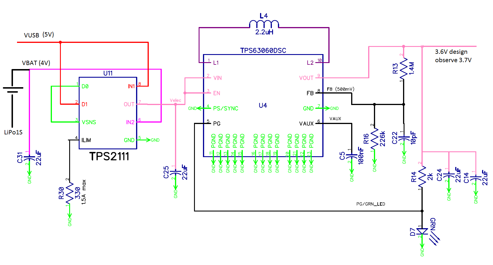
There are two mysteries at the moment - the first is that my output voltage is closer to 3.7V instead of 3.6V, and the feedback voltage is correspondingly higher than 500mV... so I haven't completely ruled out problems with the DC/DC converter design. However, this part of the circuit has worked fine for me on boards in the past and I don't see my dropout problem when I work on USB power alone.

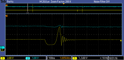
The second mystery is that the circuit fails for about 4 ms when the load is increased suddenly by driving a digital out on a downstream MCU. I'm probably asking the DC/DC converter for another ~3mA max and there are 22uF capacitors all over the place, but I do see a small drop on the input side of the DC/DC converter that suggests that for a very brief time period I am asking for a lot of current.

Some of the ideas I've thought of that don't seem to help yet:

1. Do I need a pulldown on D1 in case the dropout is caused by the TPS2111A seeing a momentary logic high and trying to switch back to USB power (which is disconnected...)

 -- I've tried adding this with some rework to no effect.

2. Is this a noise issue on one or more of the pins?

-- Hard to rule out, but the threshold voltages are all pretty high and I didn't think chip would be so finicky... no rework efforts in this direction have helped yet. Next step might be to litter the region with ferrite beads.

3. Is this an ILIM issue whereby the switch is being asked for a huge current by the DC/DC converter?

-- The datasheet isn't clear to me on what happens when the max current is exceeded. I have tried shorting Rilim to no effect -- the datasheet suggests this is "not recommended" but only mentions that the output current will not be limited.

I'm unsure what to test next. I might try soldering the pins (1,2,3, and 5) together at the package to rule out noise on the logic side.

I have verified that everything works fine off the battery if I remove the chip entirely and tie the pads 6 and 7 together to connect the battery directly to the DCDC supply... 

Any help would be greatly appreciated!


  • Hi Robb,

    We're a bit tight on resources due to the holiday season approaching. I will take a look early next week and try to respond by Tuesday (shooting for Monday).

    I'll take a look mostly from the TPS2111A's point of view. If it looks good there, I'll forward this thread to the DC/DC forum where they may have additional insight regarding the TPS63060 portion of the circuit.

    Thanks!

    Alex

  • Ok -- thank you! Happy to send traces or probe values as needed.

  • I think I am closer to understanding both the cause and a fix for my problem, but I'd still like to chase down what's likely happening with the TPS2111A.

    Here's my schematic with some test points and downstream circuits drawn in:

    My observation was that the output of the TPS2111 would switch off for about 4msec when I turned on the gate of the FET using the MCU's digital output. I had seen some small effects at testpoint (2) and thought maybe that the TPS63060 was somehow pulling too much current, or that VUSB (which is floating) might be drifting around  ... anyway I'm now pretty certain that the problem is related to noise on Vbat coming from C11 - which was intended to smooth out a PWM signal on the outputs but needs some more thought.

    In this experiment, I'm probing [1] on CH1 (at a point far away from any bypass caps and [2] on CH2, at the input capacitor near the TPS63060. The spike are from the leading and falling edge of a ~10% duty cycle PWM signal:

    zooming in on the rising edge of the first pulse:

    at the same time, the ripple on the TPS63060 is pretty much noise free and is at a much different timescale, although there is a change in the shape. Here I've moved CH2 to [3], on the output side of the TPS63060:

    For the time being, I am pulling a bunch of capacitors like C11 out of my circuit as a temporary fix...  but it would be good to know the likely cause of the dropout so I can try to protect the right pins on the TPS2111 from noise to avoid this problem in the future. Should I put a bypass near IN1 and IN2? Ferrite beads on Rilim and GND? A pull-down D1? Maybe all of the above?

    Redesigning the PWM output stage is another task... I might try adding another capacitor from Vin to GND near the high side of C11, or possibly adding a choke on the low side of C11 or between the FET source and GND.

  • Hi Robb,

    Glad to see you're making progress. I do think the input caps will help. The datasheet and EVM use 0.1uF bypass caps close to the IC pins on all diagrams and layout.

    www.ti.com/.../sbvu007.pdf
    Figure 4-1 on page 20.

    Ferrite bead on Rilim seems far overkill to me, probably not necessary. For D1, I guess a placeholder can't hurt, but I also would not think it's needed.

    By the way, just to double check I assume D0 and Vsns are connected to GND correct (not just floating)?

    Thanks,
    Alex
  • I'll probably err on the side of caution and add a bunch of passives to the next build. Do all TI products have a user's guide in addition to the datasheet? I'll certainly look for these docs in the future.

    Is there a way to understand from the block diagram in the datasheet how noise on IN1 or IN2 could lead to a drop out?

  • Maybe the internal Vdd is dropping too low and the chip is going through an enable cycle?
  • Hi Robb,

    Yes, that might be possible. I've seen cases on hot swap devices (completely different products though), where noise/fast transient on the VIN line can couple in and trigger a POR circuit, without dropping below the POR threshold voltage.

    Otherwise noise tripping the regular IN2 or IN1 UVLO thresholds circuit.

    To be honest, I have no prior experience with PMUX devices in particular. Most of our team is out for holidays, so I am filling in as I can but my background knowledge is fairly limited. My specialty is hot swap and ORing products which may have some similarities.

    After the holidays I can get in touch with some engineers who may have additional insight into these specific products and what to look out for.

    Thanks,
    Alex
  • ++ Also, it can't hurt to take a snapshot of your TPS63060 layout (and attached schematic) and ask for a review over in the non isolated DC/DC forum. They may have some layout tips to further reduce noise.

    Thanks,
    Alex
  • Ok thanks -- I appreciate your help. It's always nice to understand why things break, so if there are other insights to be had when people come back from the holidays it would be great to follow up. I'll keep an eye on the thread. Happy holidays!